Features: 512 * 18-Bit Organization Array(SN74V215)
1024 * 18-Bit Organization Array(SN74V225)
2048 * 18-Bit Organization Array(SN74V235)
4096 * 18-Bit Organization Array(SN74V245)
7.5-ns Read/Write Cycle Time
3.3-V VCC, 5-V Input Tolerant
First-Word or Standard Fall-Through Timing
Single or Double Register-Buffered Empty and Full Flags
Easily Expandable in Depth and Width
Asynchronous or Coincident Read and Write Clocks
Asynchronous or Synchronous Programmable Almost-Empty and Almost-Full Flags With Default Settings
Half-Full Flag Capability
Output Enable Puts Output Data Bus in High-Impedance State
High-Performance Submicron CMOS Technology
Packaged in 64-Pin Thin Quad Flat Package
DSP and Microprocessor Interface Control Logic
Provide a DSP Glueless Interface to Texas Instruments TMS320 DSPs
Pinout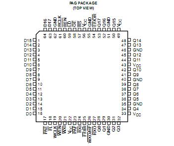 SpecificationsSupply voltage range, VCC . . . . . . . . . . . . . . . . . . . . 0.5 V to 5 V
Continuous output current, IO (VO = 0 to VCC) .. . . . . . . . ±50 mA
Storage temperature range, Tstg . . . . . . . . . . . 55°C to 125°C DescriptionThe SN74V215, SN74V225, SN74V235, and SN74V245 are very high-speed, low-power CMOS clocked first-in first-out (FIFO) memories. They support clock frequencies up to 133 MHz and have read-access times as fast as 5 ns. These DSP-Sync FIFO memories feature read and write controls for use in applications such as DSP-to-processor communication, DSP-to-analog front end (AFE) buffering, network, video, and data communications.
These SN74V215 are synchronous FIFOs, which means each port employs a synchronous interface. All data transfers through a port are gated to the low-to-high transition of a continuous (free-running) port clock by enable signals.The continuous clocks for each port are independent of one another and can be asynchronous or coincident.The enables for each port are arranged to provide a simple interface between DSPs, microprocessors, and/or
buses controlled by a synchronous interface. An output-enable (OE ) input controls the 3-state output.
The synchronous FIFOs SN74V215 have two fixed flags, empty flag/output ready (EF /OR ) and full flag/input ready (FF /IR ),and two programmable flags, almost empty (PAE ) and almost-full (PAF). The offset loading of the programmable flags is controlled by a simple state machine, and is initiated by asserting the load pin (LD). A half-full flag (HF ) is available when the FIFO is used in a single-device configuration.
Two timing modes of operation are possible with SN74V215: first-word fall-through (FWFT) mode and standard mode.
In FWFT mode, the first word written to an empty FIFO SN74V215 is clocked directly to the data output lines after three transitions of the RCLK signal. A read enable ( REN) does not have to be asserted for accessing the first word.
In SN74V215 standard mode, the first word written to an empty FIFO does not appear on the data output lines unless a specific read operation is performed. A read operation, which consists of activating REN and enabling a rising RCLK edge, shifts the word from internal memory to the data output lines.
These devices SN74V215 are depth expandable, using a daisy-chain technique or FWFT mode. The XI and XO pins are used to expand the FIFOs. In depth expansion configuration, first load ( FI) is grounded on the first device and set to high for all other devices in the daisy chain.
The SN74V215, SN74V225, SN74V235, and SN74V245 are characterized for operation from 0°C to 70°C.

 SN74V215 Data Sheet


