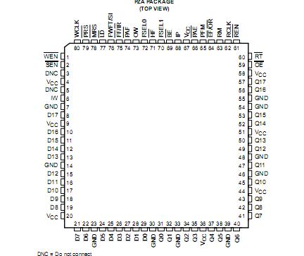
Features: Choice of Memory Organizations SN74V263 8192 * 18/16384 * 9 SN74V273 16384 * 18/32768 * 9 SN74V283 32768 * 18/65536 * 9 SN74V293 65536 * 18/131072 * 9166-MHz Operation6-ns Read/Write Cycle TimeUser-Selectable Input and Output Port Bus Sizing *9 in to *9 out *9 in to *18 out *18...
SN74V263: Features: Choice of Memory Organizations SN74V263 8192 * 18/16384 * 9 SN74V273 16384 * 18/32768 * 9 SN74V283 32768 * 18/65536 * 9 SN74V293 65536 * 18/131072 * 9166-MHz Operation6-ns Read/Wri...
SeekIC Buyer Protection PLUS - newly updated for 2013!
268 Transactions
All payment methods are secure and covered by SeekIC Buyer Protection PLUS.

The SN74V263, SN74V273, SN74V283, and SN74V293 are exceptionally deep, high-speed, CMOS first-in first-out (FIFO) memories with clocked read and write controls and a flexible bus-matching *9/*18 data flow.There is flexible *9/*18 bus matching on both read and write ports.
The period required by the retransmit operation is fixed and short.The first-word data-latency period, from the time the first word is written to an empty FIFO SN74V263 to the time it can be read, is fixed and short.
These FIFOs SN74V263are particularly appropriate for network, video, telecommunications, data communications, and other applications that need to buffer large amounts of data and match buses of unequal sizes.
Each FIFO SN74V263 has a data input port (Dn) and a data output port (Qn), both of which can assume either an 18-bit or 9-bit width, as determined by the state of external control pins' input width (IW) and output width (OW) during the master-reset cycle.
The input port is controlled by write-clock (WCLK) and write-enable ( WEN) inputs. Data is written into the FIFO SN74V263 on every rising edge of WCLK when WEN is asserted. The output port is controlled by read-clock (RCLK) and read-enable ( REN) inputs. Data is read from the FIFO on every rising edge of RCLK when REN is asserted.An output-enable ( OE) input is provided for 3-state control of the outputs.