SN751177

Features: ` Meet or Exceed the Requirements of ANSI Standards TIA/EIA-422-B and TIA/EIA-485-A and ITU Recommendations V.10 and V.11` Designed for Multipoint Bus Transmission on Long Bus Lines in Noise Environments` Driver Positive- and Negative-Current Limiting` Thermal Shutdown Protection` Driver...

product image

SN751177 Picture
SeekIC No. : 004499578 Detail

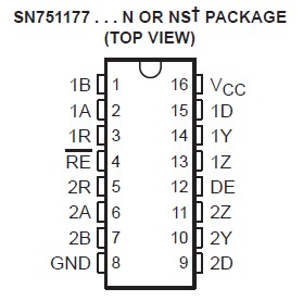
SN751177: Features: ` Meet or Exceed the Requirements of ANSI Standards TIA/EIA-422-B and TIA/EIA-485-A and ITU Recommendations V.10 and V.11` Designed for Multipoint Bus Transmission on Long Bus Lines in Noi...

floor Price/Ceiling Price
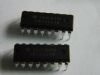
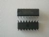
Part Number:
SN751177
Supply Ability:
5000

Price Break

  • Qty
  • 1~5000
  • Unit Price
  • Negotiable
  • Processing time
  • 15 Days
Total Cost: $ 0.00

SeekIC Buyer Protection PLUS - newly updated for 2013!

  • Escrow Protection.
  • Guaranteed refunds.
  • Secure payments.
  • Learn more >>

Month Sales

268 Transactions

Rating

evaluate  (4.8 stars)

Upload time: 2025/12/24

Payment Methods

All payment methods are secure and covered by SeekIC Buyer Protection PLUS.

Notice: When you place an order, your payment is made to SeekIC and not to your seller. SeekIC only pays the seller after confirming you have received your order. We will also never share your payment details with your seller.
Product Details

Description


Features:

` Meet or Exceed the Requirements of ANSI Standards TIA/EIA-422-B and TIA/EIA-485-A and ITU Recommendations V.10 and V.11
` Designed for Multipoint Bus Transmission on Long Bus Lines in Noise Environments
` Driver Positive- and Negative-Current Limiting
` Thermal Shutdown Protection
` Driver 3-State Outputs
` Receiver Common-Mode Input Voltage Range of 12 V to 12 V
` Receiver Input Sensitivity . . . ±200 mV
` Receiver Hysteresis . . . 50 mV Typ
` Receiver Input Impedance . . . 12 kW Min
` Receiver 3-State Outputs (SN751177 Only)
` Operate From Single 5-V Supply


Pinout

  Connection Diagram


Specifications

Supply voltage, VCC (see Note 1) . . . . . . . . . . . . . . . . . . . . . . . . . . . . . . . . . . . . . . . . . . . . .7 V
Input voltage, VI (DE, RE, and D inputs) . . . . . . . . . . . . . . . . . . . . . . . . . . . . . . . . . . . . . . . . .7 V
Receiver input voltage range, VI (A or B inputs) . . . . . . . . . . . . . . . . . . . . . . . . . .  25 V to 25 V
Receiver differential input voltage range, VID (see Note 2) . . . . . . . . . . . . . . . . . . .25 V to 25 V
Driver output voltage range, VO . . . . . . . . . . . . . . . . . . . . . . . . . . . . . . . . . . . . . . 10 V to 15 V
Receiver low-level output current, IOL . . . . . . . . . . . . . . . . . . . . . . . . . . . . . . . . . . . . . . . . 50 mA
Package thermal impedance, qJA (see Note 3): N package . . . . . . . . . . . . . . . . . . . . . . . 78°C/W
                                                                        NS package . . . . . . . . . . . . . . . . . . . . . 111°C/W
Storage temperature range, Tstg . . . . . . . . . . . . . . . . . . . . . . . . . . . . . . . . . . .65°C to 150°C
Lead temperature 1,6 mm (1/16 inch) from case for 10 seconds . . . . . . . . . . . . . . . . . . . 260°C

† Stresses beyond those listed under "absolute maximum ratings" may cause permanent damage to the device. These are stress ratings only, and
functional operation of the device at these or any other conditions beyond those indicated under "recommended operating conditions" is not implied. Exposure to absolute-maximum-rated conditions for extended periods may affect device reliability.
NOTES: 1. All voltage values, except differential input voltage, are with respect to the network ground terminal.
2. Differential input voltage is measured at the noninverting terminal with respect to the inverting terminal.
3. The package thermal impedance is calculated in accordance with JESD 51, except for through-hole packages, which use a trace length of zero.


Description

The SN751177 and SN751178 dual differential drivers and receivers are monolithic integrated circuits that are designed for balanced multipoint bus transmission at rates up to 10 Mbit/s. They are designed to improve the performance of full-duplex data communications over long bus lines and meet ANSI Standards TIA/EIA-422-B and TIA/EIA-485-A and ITU Recommendations V.10 and V.11.

The SN751177 and SN751178 driver outputs provide limiting for both positive and negative currents and thermal-shutdown protection from line-fault conditions on the transmission bus line.

The receiver SN751177 features high input impedance of at least 12 kW, an input sensitivity of ±200 mV over a common-mode input voltage range of 12 V to 12 V, and typical input hysteresis of 50 mV. Fail-safe design ensures that if the receiver inputs are open, the receiver outputs always will be high.

The SN751177 and SN751178 are characterized for operation from 20°C to 85°C.


Customers Who Bought This Item Also Bought

Margin,quality,low-cost products with low minimum orders. Secure your online payments with SeekIC Buyer Protection.
Soldering, Desoldering, Rework Products
Computers, Office - Components, Accessories
Fans, Thermal Management
Test Equipment
Resistors
View more