Application Characterized for Use to 300 mA
High-Voltage Outputs
No Output Latch-Up at 55 V (After Conducting 300 mA)
Medium-Speed Switching
Circuit Flexibility for Varied Applications and Choice of Logic Function
TTL-Compatible Diode-Clamped Inputs
Standard Supply Voltages
Plastic DIP (P) With Copper Lead Frame Provides Cooler Operation and Improved ReliabilityPinout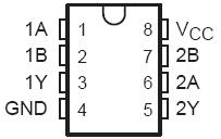 Specifications
Supply voltage, VCC (see Note 1) . . . . . . . . . . . . . . . . . . . . . . . . . . . . . . . . . . . . . . . . . . . . . . . . . . . . . . . . . . 7 V
Input voltage, VI . . . . . . . . . . . . . . . . . . . . . . . . . . . . . . . . . . . . . . . . . . . . . . . . . . . . . . . . . . . . . . . . . . . . . 5.5 V
Inter-emitter voltage (see Note 2) . . . . . . . . . . . . . . . . . . . . . . . . . . . . . . . . . . . . . . . . . . . . . . . . . . . . . . . .5.5 V
Off-state output voltage, VO . . . . . . . . . . . . . . . . . . . . . . . . . . . . . . . . . . . . . . . . . . . . . . . . . . . . . . . . . . . . 70 V
Continuous collector or output current (see Note 3) . . . . . . . . . . . . . . . . . . . . . . . . . . . . . . . . . . . . . . . . 400 mA
Peak collector or output current (tw 3 10 ms, duty cycle 3 50%, see Note 3) . . . . . . . . . . . . . . . . . . . . . 500 mA
Continuous total power dissipation . . . . . . . . . . . . . . . . . . . . . . . . . . . . . . . . . . . . See Dissipation Rating Table
Operating free-air temperature range, TA . . . . . . . . . . . . . . . . . . . . . . . . . . . . . . . . . . . . . . . . . . ..0°C to 70°C
Storage temperature range, Tstg . . . . . . . . . . . . . . . . . . . . . . . . . . . . . . . . . . . . . . . . . . . . . . 65°C to 150°C
Lead temperature 1,6 mm (1/16 inch) from case for 10 seconds . . . . . . . . . . . . . . . . . . . . . . . . . . . . . . . 260°C
NOTES: 1. Voltage values are with respect to the network GND, unless otherwise specified.
2. This is the voltage between two emitters, A and B.
3. Both halves of these dual circuits may conduct rated current simultaneously; however, power dissipation averaged over a short time interval must fall within the continuous dissipation rating.
DescriptionSeries SN75472 dual peripheral drivers are functionally interchangeable with series SN75451B and series SN75461 peripheral drivers, but are designed for use in systems that require higher breakdown voltages than either of those series can provide at the expense of slightly slower switching speeds than series 75451B (limits are the same as series SN75461). Typical applications include high-speed logic buffers, power drivers, relay drivers, lamp drivers, MOS drivers, line drivers, and memory drivers.
The SN75471, SN75472, and SN75473 are dual peripheral AND, NAND, and OR drivers, respectively, (assuming positive logic), with the output of the logic gates internally connected to the bases of the npn output transistors. Series SN75471 drivers are characterized for operation from 0°C to 70°C.

 SN75472 Data Sheet