DescriptionThe SN75497 is designed as MOS-to-LED 7-channel driver which is to drive common-cathode LED's in serially addressed multi-digit displays used in conjunction with MOS calculator circuits. The input of each circuit is capable of interfacing with an MOS push-pull output buffer while the ou...
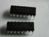
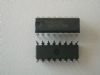
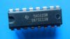
SN75497: DescriptionThe SN75497 is designed as MOS-to-LED 7-channel driver which is to drive common-cathode LED's in serially addressed multi-digit displays used in conjunction with MOS calculator circuits. ...
SeekIC Buyer Protection PLUS - newly updated for 2013!
268 Transactions
All payment methods are secure and covered by SeekIC Buyer Protection PLUS.
The SN75497 is designed as MOS-to-LED 7-channel driver which is to drive common-cathode LED's in serially addressed multi-digit displays used in conjunction with MOS calculator circuits. The input of each circuit is capable of interfacing with an MOS push-pull output buffer while the output is capable of sinking the output current from a strobed LED display.
SN75497 has seven features. (1)100mA output sink current capability. (2)Low voltage operation. (3)MOS- and TTL-compatible inputs. (4)Input threshold 2.7V max. (5)7 drivers per package. (6)Low-voltage saturating outputs. (7)Low standby power. Those are all the main features.
Some SN75497 absolute maximum ratings have been concluded into several points as follow. (1)Its input voltage would be from -11V to Vcc. (2)Its output voltage would be Vcc. (3)Its continuous output collector current would be 125uA. (4)Its ground-terminal current would be 250uA. (5)Its continuous total dissipation over entire operating range would be 500mW. (6)Its operating free-air temperature range would be from 0°C to 70°C. (7)Its storage temperature range would be from -65°C to 150°C. (8)Its lead temperature 1/16 inch from case for 10 seconds would be 260°C. It should be noted that stresses above those listed in absolute maximum ratings may cause permanent damage to device.
Also some SN75497 electrical characteristics are concluded as follow. (1)Its off-state output current would be typ 10uA and max 100uA. (2)Its on-state output voltage would be typ 0.24V and max 0.4V at Vcc=6.6V and would be typ 0.12V and max 0.4V at Vcc=2.7V and Io=50mA. (3)Its high level input current would be typ 0.6mA and max 1mA at Vcc=6.6V and would be max 0.4mA at Vcc=2.7V. (4)Its low-level input current would be typ -10ua and max -100uA at Vcc=6.6V and would be max -100uA at Vcc=2.7V. (5)Its supply current would be typ 2.5mA and max 5mA at one driver on and would be max 200uA for all drivers off. And so on. If you have any question or suggestion or want to know more information please contact us for details. Thank you!