SN75C1154

Features: *Meet or Exceed the Requirements of TIA/EIA-232-F and ITU Recommendation V.28*Very Low Power Consumption...5 mW Typ*Wide Driver Supply Voltage...±4.5 V to ±15 V*Driver Output Slew Rate Limited to 30 V/s Max*Receiver Input Hysteresis ...1000 mV Typ*Push-Pull Receiver Outputs*On-Chip Recei...

product image

SN75C1154 Picture
SeekIC No. : 004499695 Detail

SN75C1154: Features: *Meet or Exceed the Requirements of TIA/EIA-232-F and ITU Recommendation V.28*Very Low Power Consumption...5 mW Typ*Wide Driver Supply Voltage...±4.5 V to ±15 V*Driver Output Slew Rate Lim...

floor Price/Ceiling Price

Part Number:
SN75C1154
Supply Ability:
5000

Price Break

  • Qty
  • 1~5000
  • Unit Price
  • Negotiable
  • Processing time
  • 15 Days
Total Cost: $ 0.00

SeekIC Buyer Protection PLUS - newly updated for 2013!

  • Escrow Protection.
  • Guaranteed refunds.
  • Secure payments.
  • Learn more >>

Month Sales

268 Transactions

Rating

evaluate  (4.8 stars)

Upload time: 2025/12/24

Payment Methods

All payment methods are secure and covered by SeekIC Buyer Protection PLUS.

Notice: When you place an order, your payment is made to SeekIC and not to your seller. SeekIC only pays the seller after confirming you have received your order. We will also never share your payment details with your seller.
Product Details

Description


Features:

*Meet or Exceed the Requirements of
  TIA/EIA-232-F and ITU Recommendation V.28
*Very Low Power Consumption...5 mW Typ
*Wide Driver Supply Voltage...±4.5 V to ±15 V
*Driver Output Slew Rate Limited to 30 V/s Max
*Receiver Input Hysteresis ...1000 mV Typ
*Push-Pull Receiver Outputs
*On-Chip Receiver 1-s Noise Filter


Application

Audio
Automotive
Broadband
Digital Control
Military
Optical Networking
Security
Telephony
Video & Imaging
Wireless


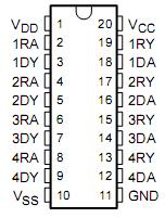
Pinout

  Connection Diagram


Specifications

Supply voltage:VDD (see Note 1) . . . . .. . . .. .. . . . .. .. . .. . . .. ..  .. . .15 V
                        VSS. . . . . . . .. .. . . . .. .. . . . .. .. . . . .. .. . . . .. .. . . . .. -15 V
                        VCC . .. . . .. .. . . . .. .. . . . .. .. . . . .. .. . . . .. .. . . . .. ..  . .7V
Input voltage range, VI:Driver . . . . . . .. .. . . . .. .. . . . .. . . .. . .VSS TO VDD
                                      Receiver  . . . . .. .. . . . .. .. . . . .. . . . -30 V to 30 V
Onput voltage range, VO:Driver . . . . . . . .. .. . .. .. . .(VSS -6V)TO (VDD+6V)
                                       Receiver  . .. . . .. .. . . . .. . . . -0.3V to (VCC+0.3V)

Package thermal impedance, JA (see Notes 2 and 3):
                                               DW package. . . . . . .. .. . . . .. .. . .. . 58/W
                                               N package  . . . . ... . . .. .. . . . .. . . .  69/W
                                               NS package . . . . ... . . .. .. . . . .. . . . 60/W
Operating virtual junction temperature, TJ. . . . .. .. .. . . .. .. . . . .. .  .150
Storage temperature range, Tstg . . . .. .. .. . .. ..  . .. ..  . ..  .-65 to 150
Lead temperature 1,6 mm (1/16 inch) from case for 10 seconds.. .. 260


Description

    The SN65C1164 and SN75C1154 are low-power BiMOS devices containing four independent drivers and receivers that are used to interface data terminal equipment (DTE) with data circuit-terminating equipment (DCE). These devices are designed to conform to TIA/EIA-232-F. The drivers and receivers of the SN65C1154 and SN75C1154 are similar to those of the SN75C188 quadruple driver and SN75C189A quadruple receiver, respectively. The drivers have a controlled output slew rate that is limited to a maximum of 30 V/s and the receivers have filters that reject input noise pulses of shorter than 1s. Both these features eliminate the need for external components.

    The SN65C1154 and SN75C1154 have been designed using low-power techniques in a BiMOS technology. In most applications, the receivers contained in these devices interface to single inputs of peripheral devices such as ACEs, UARTs, or microprocessors. By using sampling, such peripheral devices usually are insensitive to the transition times of the input signals. If this is not the case, or for other uses, it is recommended that the SN65C1154 and SN75C1154 receiver outputs be buffered by single Schmitt input gates or single gates of the HCMOS, ALS, or 74F logic families.


Customers Who Bought This Item Also Bought

Margin,quality,low-cost products with low minimum orders. Secure your online payments with SeekIC Buyer Protection.
Circuit Protection
Power Supplies - Board Mount
Discrete Semiconductor Products
Isolators
Semiconductor Modules
View more