Features: ` Designed for TIA/EIA-485, TIA/EIA-422, and ISO 8482 Applications
` Signaling Rate† Exceeding 50 Mbps
` Fail-Safe in Bus Short-Circuit, Open-Circuit, and Idle-Bus Conditions
` ESD Protection on Bus Inputs Exceeds 6 kV
` Common-Mode Bus Input Range 7 V to 12 V
` Propagation Delay Times <16 ns
` Low Standby Power Consumption <20 mA
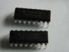
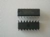
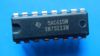
` Pin-Compatible Upgrade for AM26LS32, DS96F173, LTC488, and SN75173Pinout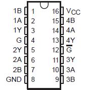 Specifications
Supply voltage range, VCC (see Note 1) . . . . . . . . . . . . . . . . . . . . . . . . . . . . . . . . . . . . . 0.3 V to 6 V
Voltage range at any bus input (DC) . . . . . . . . . . . . . . . . . . . . . . . . . . . . . . . . . . . . . . . 10 V to 15 V
Voltage range at any bus input (transient pulse through 100 W, see Figure 5) . . . . . . 30 V to 30 V
Voltage input range at G and G, VI . . . . . . . . . . . . . . . . . . . . . . . . . . . . . . . . . . 0.5 V to VCC + 0.5 V
Electrostatic discharge:
Human body model (see Note 2): A and B to GND . . . . . . . . . . . . . . . . . . . . . . . . . . . . . . . . . . . 6 kV
All pins . . . . . . . . . . . . . . . . . . . . . . . . . . . . . . . . . . . . .. . . . . . . 5 kV
Charged-device model (see Note 3): All pins . . . . . . . . . . . . . . . . . . . . . . . . . . . . . . . . . . . . . . . 2 kV
Storage temperature range . . . . . . . . . . . . . . . . . . . . . . . . . . . . . . . . . . . . . . . . .. . 65°C to 150°C
Continuous power dissipation . . . . . . . . . . . . . . . . . . . . . . . . . . .. See Power Dissipation Rating Table
Lead temperature 1,6 mm (1/16 inch) from case for 10 seconds . . . . . . . . . .. . . . . . . . . . . . . . 260°C
† Stresses beyond those listed under "absolute maximum ratings" may cause permanent damage to the device. These are stress ratings only, and functional operation of the device at these or any other conditions beyond those indicated under "recommended operating conditions" is not implied. Exposure to absolute-maximum-rated conditions for extended periods may affect device reliability.
NOTES: 1. All voltage values, except differential I/O bus voltages, are with respect to GND, and are steady-state (unless otherwise specified).
2. Tested in accordance with JEDEC Standard 22, Test Method A114-A.
3. Tested in accordance with JEDEC Standard 22, Test Method C101.
DescriptionThe SN65LBC173A and SN75LBC173A are quadruple differential line receivers with 3-state outputs, designed for TIA/EIA-485 (RS-485), TIA/EIA-422 (RS-422), and ISO 8482 (Euro RS-485) applications.
These devices SN75LBC173A are optimized for balanced multipoint bus communication at data rates up to and exceeding 50 million bits per second. The transmission media may be twisted-pair cables, printed-circuit board traces, or backplanes. The ultimate rate and distance of data transfer is dependent upon the attenuation characteristics of the media and the noise coupling to the environment.
Each receiver operates over a wide range of positive and negative common-mode input voltages, and features ESD protection to 6 kV, making it suitable for high-speed multipoint data transmission applications in harsh environments. These devices SN75LBC173A are designed using LinBiCMOS�, facilitating low power consumption and robustness.
The SN75LBC173A G and G inputs provide enable control logic for either positive- or negative-logic enabling all four drivers. When disabled or powered off, the receiver inputs present a high-impedance to the bus for reduced system loading.
The SN75LBC173A is characterized for operation over the temperature range of 0°C to 70°C. The SN65LBC173A is characterized over the temperature range from 40°C to 85°C.

 SN75LBC173A Data Sheet