SN75LBC176A

Features: High-Speed Low-Power LinBiCMOSTMCircuitry Designed for Signaling Rates† Upto 30 MbpsBus-Pin ESD Protection Exceeds 12 kVHBMCompatible With ANSI StandardTIA/EIA-485-A and ISO 8482:1987(E)Low SkewDesigned for Multipoint Transmission onLong Bus Lines in Noisy EnvironmentsVery Low Disa...

product image

SN75LBC176A Picture
SeekIC No. : 004499736 Detail

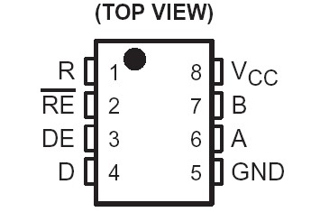
SN75LBC176A: Features: High-Speed Low-Power LinBiCMOSTMCircuitry Designed for Signaling Rates† Upto 30 MbpsBus-Pin ESD Protection Exceeds 12 kVHBMCompatible With ANSI StandardTIA/EIA-485-A and ISO 8482:198...
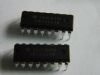
floor Price/Ceiling Price

Part Number:
SN75LBC176A
Supply Ability:
5000

Price Break

  • Qty
  • 1~5000
  • Unit Price
  • Negotiable
  • Processing time
  • 15 Days
Total Cost: $ 0.00

SeekIC Buyer Protection PLUS - newly updated for 2013!

  • Escrow Protection.
  • Guaranteed refunds.
  • Secure payments.
  • Learn more >>

Month Sales

268 Transactions

Rating

evaluate  (4.8 stars)

Upload time: 2025/12/24

Payment Methods

All payment methods are secure and covered by SeekIC Buyer Protection PLUS.

Notice: When you place an order, your payment is made to SeekIC and not to your seller. SeekIC only pays the seller after confirming you have received your order. We will also never share your payment details with your seller.
Product Details

Description


Features:

High-Speed Low-Power LinBiCMOSTMCircuitry Designed for Signaling Rates† Upto 30 Mbps
Bus-Pin ESD Protection Exceeds 12 kVHBM
Compatible With ANSI StandardTIA/EIA-485-A and ISO 8482:1987(E)
Low Skew
Designed for Multipoint Transmission onLong Bus Lines in Noisy Environments
Very Low Disabled Supply-CurrentRequirements . . . 700 µA Maximum
Common Mode Voltage Range of −7 Vto 12 V
Thermal-Shutdown Protection
Driver Positive and Negative CurrentLimiting
Open-Circuit Fail-Safe Receiver Design
Receiver Input Sensitivity . . . ±200 mV Max|
Receiver Input Hysteresis . . . 50 mV Typ
Glitch-Free Power-Up and Power-DownProtection
Available in Q-Temp AutomotiveHigh Reliability Automotive ApplicationsConfiguration Control / Print SupportQualification to Automotive Standards


Pinout

  Connection Diagram


Specifications

Supply voltage, VCC (see Note 1)  . . . . . . . . . . . . . . . . . . .  . . . . . . . . . . . .  . . . . . . . . . .−0.3 V to 6 V
Voltage range at any bus terminal (A or B)  . . . . . . . . . . . . . . . .. . . . . . . . . .. . . . . . . . . −10 V to 15 V
Input voltage, VI (D, DE, R, or RE ). . . . . . . . . . . . . . . . . . . . . . . . . . . .. . . . . .  . . −0.3 V to VCC + 0.5 V
Electrostatic discharge: Bus terminals and GND, Class 3, A: (see Note 2) . . . .  . . . . . . . . . . . . . .12 kV
                                      Bus terminals and GND, Class 3, B: (see Note 2)  . . . . . . . . . . . . . . . . . .400 V
                                      All terminals, Class 3, A: . . . . . . . . . . . . . . . . . . . . . . . . . . . . . . . . . . . . . . 3 kV
                                      All terminals, Class 3, B:  . . . . . . . . . . . . . . . . . . . . . . . . . . . . . . . . . . . . .400 V
Continuous total power dissipation (see Note 3)  . . . . . . . .. . . . . . . . . . . .See Dissipation Rating Table
Storage temperature range, Tstg . . . . . . . . . . . . . . . . . . . . . . . . . . . . . . . . . . . . . . . . . . .−65 to 150
Lead temperature 1,6 mm (1/16 inch) from case for 10 seconds . . . . . . . . . . . . . . . . .  . . . . . . . . .260


Description

The SN65LBC176A, SN65LBC176AQ, andSN75LBC176A differential bus transceivers aremonolithic, integrated circuits designed forbidirectional data communication on multipointbus-transmission lines. They are designed forbalanced transmission lines and are compatiblewith ANSI standard TIA/EIA-485-A and ISO 8482.The A version offers improved switching performanceover its predecessors without sacrificingsignificantly more power.

The SN65LBC176A, SN65LBC176AQ, and SN75LBC176A combine a 3-state, differential line driver and adifferential input line receiver, both of which operate from a single 5-V power supply. The driver and receiverhave active-high and active-low enables, respectively, which can externally connect together to function as adirection control. The driver differential outputs and the receiver differential inputs connect internally to form adifferential input/output (I/O) bus port that is designed to offer minimum loading to the bus whenever the driveris disabled or VCC = 0. This port features wide positive and negative common-mode voltage ranges, making the device SN75LBC176A suitable for party-line applications. Very low device supply current can be achieved by disabling thedriver and the receiver.


Customers Who Bought This Item Also Bought

Margin,quality,low-cost products with low minimum orders. Secure your online payments with SeekIC Buyer Protection.
Isolators
Hardware, Fasteners, Accessories
Programmers, Development Systems
Boxes, Enclosures, Racks
Semiconductor Modules
Memory Cards, Modules
View more