Features: ` Operates With Single 5-V Power Supply
` Meets or Exceeds the Requirements of TIA/EIA-232-F and ITU Recommendation V.28
` Improved Performance Replacement for MAX241
` Operates at Data Rates up to 100 kbit/s Over a 3-m Cable
` Low-Power Shutdown Mode . . . 1 A Typ
` LinBiCMOSE Process Technology
` Four Drivers and Five Receivers
` ±30-V Input Levels
` 3-State TTL/CMOS Receiver Outputs
` ±9-V Output Swing With a 5-V Supply
` Applications
TIA/EIA-232-F Interface
Battery-Powered Systems
Terminals
Modems
Computers
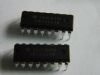
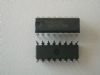
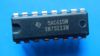
` Package Options Include Plastic Small-Outline (DW) and Shrink Small-Outline (DB) PackagesPinout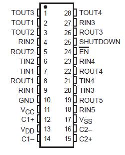 Specifications
Input supply voltage range, VCC (see Note 1) . . . . . . . . . . . . . . . . . . . . . . . . . . . .. . . . . . . . 0.3 V to 6 V
Positive output supply voltage range, VDD . . . . . . . . . . . . . . . . . . . . . . . . . . . . . . . . . VCC 0.3 V to 15 V
Negative output supply voltage range, VSS . . . . . . . . . . . . . . . . . . . . . . . . . . . . . . . . . . . . 0.3 V to 15 V
Input voltage range, VI: Driver . . . . . . . . . . . . . . . . . . . . . . . . . . . . . . . . . . . . . . . . 0.3 V to VCC + 0.3 V
Receiver . . . . . . . . . . . . . . . . . . . . . . . . . . . . . . . . . . . . . .. . . . . . . . . . . . . ±30 V
Output voltage range, VO: TOUT . . . . . . . . . . . . . . . . . . . . . . . . . . . . . . . . . . VSS 0.3 V to VDD + 0.3 V
ROUT . . . . . . . . . . . . . . . . . . . . . . . . . . . . . . . . . . . . . . 0.3 V to VCC + 0.3 V
Short-circuit duration: TOUT . . . . . . . . . . . . . . . . . . . . . . . . . . . . . . . . . . . . . . . . . . . . . . . . . . . . Unlimited
Continuous total dissipation . . . . . . . . . . . . . . . . . . . . . . . . . . . . . . . . . . .. . See Dissipation Rating Table
Storage temperature range, Tstg . . . . . . . . . . . . . . . . . . . . . . . . . . . . . . . . . . . . . . . . . 65°C to 150°C
Lead temperature 1,6 mm (1/16 inch) from case for 10 seconds . . . . . . . . . . . . . . . . . .. . . . . . . . 260°C
† Stresses beyond those listed under "absolute maximum ratings" may cause permanent damage to the device. These are stress ratings only, and functional operation of the device at these or any other conditions beyond those indicated under "recommended operating conditions" is not implied. Exposure to absolute-maximum-rated conditions for extended periods may affect device reliability.
NOTE 1: All voltage values are with respect to the network ground terminal.
DescriptionThe SN75LBC241† is a low-power LinBiCMOSE line-interface device containing four independent drivers and five receivers. It is designed as a plug-in replacement for the Maxim MAX241. The SN75LBC241 provides a capacitive-charge-pump voltage generator to produce RS-232 voltage levels from a 5-V supply. The charge-pump oscillator frequency is 20 kHz. Each receiver converts RS-232 inputs to 5-V TTL/CMOS levels. The receivers have a typical threshold of 1.2 V and a typical hysteresis of 0.5 V and can accept ±30-V inputs. Each driver converts TTL/CMOS input levels into RS-232 levels.
The SN75LBC241 includes a receiver, a 3-state control line, and a low-power shutdown control line. When the EN line is high, receiver outputs are placed in the high-impedance state. When EN is low, normal operation is enabled.
The SN75LBC241 shutdown mode reduces power dissipation to less than 5 mW typically. In this mode, receiver outputs have high impedance, driver outputs are turned off, and the charge-pump circuit is turned off. When SHUTDOWN is high, the shutdown mode is enabled. When SHUTDOWN is low, normal operation is enabled.
This device SN75LBC241 has been designed to conform to TIA/EIA-232-F and ITU Recommendation V.28.
The SN75LBC241 has been designed using LinBiCMOS technology and cells contained in the Texas Instruments LinASICE library. Use of LinBiCMOS circuitry increases latch-up immunity in this device over an all-CMOS design.
The SN75LBC241 is characterized for operation from 0°C to 70°C.

 SN75LBC241 Data Sheet