Pinout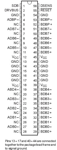 SpecificationsSupply voltage range, VCC (see Note 1) . . . . . . . . . . . . . . . . . . . . . . . . . . . . . . . . . . . . . 0.3 V to 7 V
Differential bus voltage range (B side) . . . . . . . . . . . . . . . . . . . . . . . . .. . . . . . . . . . . . . . 15 V to 15 V
Single-ended bus voltage range (A side and control inputs) . . . . . . . ......... . . . . . . . . . . 0.3 V to 7 V
Continuous total power dissipation (see Note 2) . . . . Internally Limited (see Dissipation Rating Table)
Electrostatic discharge (see Note 3): Class 1 A (all pins) . . . . . . .. . . . . . . . . . . . . . . . . . . . . . . . . 500 V
Class 1 B (all pins) . . . . . . . . . . . . . . . . . . . . . . . . . . . . . . . . . . . . . . 200 V
Class 2 A (B-side and GND) . . . . . . . . ... . . . . . . . . . . . . . . . . . . . . . . 2 kV
Class 2 B (B-side and GND) . . . . . . . ... . . . . . . . . . . . . . . . . . . . . . . 200 V
Operating free-air temperature range, TA . . . . . . . . . . . . . . . . . . . . . . . . . . . . . . . . . . . . . 0oC to 70 oC
Storage temperature range, Tstg . . . . . . . . . . . . . . . . . . . . . . . . . . . . . . . . . . . . . . . . . . 65oC to 150oC
Lead temperature 1,6 mm (1/16 inch) from case for 10 seconds . . . .. . . . . . . . . . . . . . . . . . . . . 260°CDescriptionThe SN75LBC971A SCSI differential converter-data is an adaptation of the industry's first 9-channel RS-485 transceiver, the SN75LBC976. When used in conjunction with its companion control transceiver, the SN75LBC970A, the resulting chip set provides the superior electrical performance of differential SCSI from a single-ended SCSI bus or controller. A 16-bit SCSI bus can be implemented with just three devices (two data and one control) in the space efficient, 56-pin, shrink small-outline package (SSOP) and a few external components. An 8-bit SCSI bus requires only one data and one control transceiver.
In a typical differential SCSI node, the SCSI controller provides an enable for each external RS-485 transceiver channel. This could require as many as 27 extra terminals for a 16-bit differential bus controller or relegate a 16-bit, single-ended controller to only an 8-bit differential bus. Using the standard nine SCSIcontrol signals, the SN75LBC970A control transceiver decodes the state of the bus and enables the SN75LBC971A data transceiver to transmit the single-ended SCSI input signals (A side) differentially to the cable or receive the differential cable signals (B side) and drive the single-ended outputs to the controller.
A SN75LBC971A reset function, which disables all outputs and clears internal latches, can be accomplished from two external inputs and two internally-generated signals. RESET (reset) and DSENS (differential sense) are available to external circuits for a bus reset or to disable all outputs should a single-ended cable be inadvertently connected to a differential connector. Internally-generated power-up and thermal-shutdown signals have the same affectwhen the supply voltage is below approximately 3.5 V or the junction temperature exceeds 175°C.
The SCSI SN75LBC971A, differential, converter-data chip operates in two modes depending on the state of the DRVBUS input.With DRVBUS low, a bidirectional latch circuit sets the direction of data transfer. Each data bit has its own latch,and each bit's direction is independent of all other bits. When neither the single-ended nor the differential sides are asserted, the latch disables both A- and B-side output drivers. When the input to either side is asserted, the latch enables the opposite side's driver and sets data flow from the asserted input to the opposite side of the device SN75LBC971A. When the input deasserts, the latch maintains the direction until the receiver on the enabled driver detects a deassertion. The latch then returns to the initial state. No parity checking is done by this device; the parity signal passes through the device like other data signals do.
About the SN75LBC971A,When DRVBUS is high, direction is determined by the SDB signal. However, a change in SDB does not always immediately change the direction. When DRVBUS first asserts, the direction indicated by SDB is latched and takes effect immediately. When SDB changes while DRVBUS is high, the drivers that were on immediately turn off. However, the other driver set does not turn on until the receivers sense a deasserted state on all nine data lines. This is done to prevent the active drivers from turning on until all other drivers are off and the terminators pull the lines to a deasserted state.
The single-ended SCSI bus interface SN75LBC971A consists of CMOS, bidirectional inputs and outputs. The drivers are rated to ±16 mA of output current. The receiver inputs are pulled high with approximately 4 mA to eliminate the need for external pullup resistors for the open-drain outputs of most single-ended SCSI controllers. The single-ended side of the device is not intended to drive the SCSI bus directly.
The differential SCSI bus interface SN75LBC971A consists of bipolar, bidirectional inputs and outputs that meet or exceed the requirements of EIA-485 and ISO 8482-1982/TIA TR30.2 referenced by American National Standard of Information Systems (ANSI) X3.131-1994 Small Computer System Interface-2 (SCSI-2).
The SN75LBC971A is characterized for operation over the temperature range of 0°C to 70°C.

 SN75LBC971A Data Sheet