Features: ` Single-Chip TIA/EIA-232-F Interface for IBMTM PC/ATTM Serial Port
` Designed to Transmit and Receive 4-ms Pulses (Equivalent to 256 kbit/s)
` Less Than 21-mW Power Consumption
` Wide Supply-Voltage Range, 4.75 V to 15 V
` Driver Output Slew Rates Are Internally Controlled to 30 V/ms Max
` Receiver Input Hysteresis, 1000 mV Typ
` TIA/EIA-232-F Bus-Pin ESD Protection Exceeds:
15-kV, Human-Body Model
IEC1000-4-2 Level-4 Compliant
` Three Drivers and Five Receivers Meet or Exceed the Requirements of TIA/EIA-232-F and ITU V.28
` Complements the SN75LP196
` Designed to Replace the Industry-Standard SN75185 and SN75C185 With the Same Flow-Through Pinout
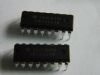
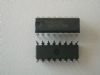
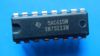
` Package Options Include Plastic Small-Outline (DW), Shrink Small-Outline (DB), Thin Shrink Small-Outline (PW), and Dual-In-Line (N) PackagesPinout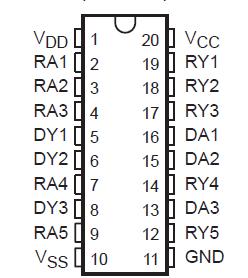 Specifications
Positive supply-voltage range (see Note 1): VCC.........................0.5 V to 7 V
VDD ................................................0.5 V to 15 V
Negative supply-voltage range, VSS (see Note 1)........................0.5 V to 15 V
Input-voltage range, VI: Receiver (RA) ............................. 30 V to 30 V
Driver (DA)........................................ 0.5 V to VCC + 0.4 V
Output-voltage range, VO: Receiver (RY) .............................0.5 V to 6 V
Driver (DY) ............................................15 V to 15 V
Electrostatic discharge: Bus pins (human-body model) (see Note 2) .............. Class 3: 15 kV
Bus pins (machine model)......................................... 500 V
Bus pins (IEC1000-4-2, contact) ...................................... 8 kV
All pins (human-body model) (see Note 2) ............................ Class 3: 5 kV
All pins (machine model)..........................................400 V
Package thermal impedance, qJA (see Note 3): DB package .....................115°C/W
DW package ..............................................97°C/W
N package ............................................... 67°C/W
PW package ............................................. 128°C/W
Storage temperature range, Tstg ................................65°C to 150°C
Lead temperature 1,6 mm (1/16 inch) from case for 10 seconds .....................260°C
†Stresses beyond those listed under "absolute maximum ratings" may cause permanent damage to the device. These are stress ratings only, and functional operation of the device at these or any other conditions beyond those indicated under "recommended operating conditions" is not implied. Exposure to absolute-maximum-rated conditions for extended periods may affect device reliability.
NOTES:
1. All voltage values are with respect to network ground terminal, unless otherwise noted.
2. Per MIL-STD-883, Method 3015.7
3. The package thermal impedance is calculated in accordance with JESD 51, except for through-hole packages, which use a trace
length of zero.
DescriptionThe SN75LP1185 is a low-power bipolar device containing three drivers and five receivers with 15 kV of ESD protection on the bus pins with respect to each other. Bus pins are defined as those pins that tie directly to the serial-port connector, including GND. The pinout matches the flow-through design of the industry-standard SN75185 and SN75C185. The flow-through pinout of the device allows easy interconnection of the UART and serial-port connector of the IBM PC/AT and compatibles. The SN75LP1185 provides a rugged, low-cost solution for this function with the combination of the bipolar processing and 15 kV of ESD protection.
The SN75LP1185 has internal slew-rate control to provide a maximum rate of change in the output signal of 30 V/ms. The driver output swing is nominally clamped at ±6 V to enable the higher data rates associated with this device and to reduce EMI emissions. Even though the driver outputs are clamped, they can handle voltages up to ±15 V without damage. All the logic inputs can accept 3.3-V or 5-V input signals.
The SN75LP1185 complies with the requirements of TIA/EIA-232-F and ITU V.28. These standards are for data interchange between a host computer and peripheral at signaling rates up to 20 kbit/s. The switching speeds of the device support rates up to 256 kbit/s.
The SN75LP1185 is characterized for operation from 0°C to 70°C.

 SN75LP1185 Data Sheet