Features: ` Single-Chip RS-232 Interface for IBM™ PC™ Compatible Serial Port` Designed to Transmit and Receive 4-s Pulses(Equivalent to 256 kbit/s)` Standby Power Is Less Than 750 W Maximum` Wide Supply-Voltage Range . . . 4.75 V to 15 V` Driver Output Slew Rates Are Internally Control...
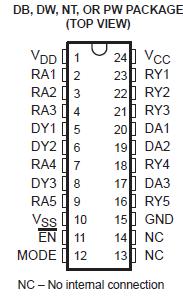
SN75LPE185: Features: ` Single-Chip RS-232 Interface for IBM™ PC™ Compatible Serial Port` Designed to Transmit and Receive 4-s Pulses(Equivalent to 256 kbit/s)` Standby Power Is Less Than 750 W Maxi...
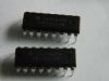
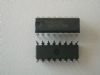
SeekIC Buyer Protection PLUS - newly updated for 2013!
268 Transactions
All payment methods are secure and covered by SeekIC Buyer Protection PLUS.

The SN75LPE185 is a low-power bipolar device containing three drivers and five receivers, with 15-kV ESD protection on the bus pins, with respect to each other. Bus pins are defined as those pins that tie directly to the serial-port connector, including GND. The pinout matches the flow-through design of the industry-standard SN75185, SN75C185, and SN75LP185, with the addition of four pins for control signals. The flow-through pinout of the device allows easy interconnection of the UART and serial-port connector of the IBM PC compatibles. The SN75LPE185 provides a rugged, low-cost solution for this function with the combination of bipolar processing and 15-kV ESD protection.
The SN75LPE185 has an internal slew-rate control to provide a maximum rate of change in the output signal of 30 V/ms. The driver output swing is clamped at ±6 V to enable the higher data rates associated with this device and reduce EMI emissions. Although the driver outputs are clamped, the outputs can handle voltages up to ±15 V without damage.
The device SN75LPE185 has flexible control options for power management when the serial port is inactive. A common disable for all of the drivers and receivers is provided with the active-low enable (EN) input. The mode control (MODE) input selects between the STANDBY and WAKE-UP modes. With a low-level input on the MODE pin and a high-level input on the EN pin, one receiver remains active while the remaining drivers and receivers are disabled to implement the WAKE-UP mode. With a high-level input on both the MODE and EN pins, all drivers and receivers are disabled to implement the STANDBY mode. The outputs of the drivers are in a high-impedance state when the device is powered off. To ensure the outputs of the receivers are in a known
output level (as listed in the Application Information section of this data sheet) when the device SN75LPE185 is powered off, in STANDBY, or WAKE-UP mode, external pullup/pulldown circuitry must be provided. All the logic inputs accept 3.3-V or 5-V input signals.
The SN75LPE185 complies with the requirements of TIA/EIA-232-F and ITU v.28 standards. These standards are for data interchange between a host computer and peripheral at signaling rates up to 20 kbit/s. The switching speeds of the device support rates up to 256 kbit/s.
The SN75LPE185 is characterized for operation from 0°C to 70°C.