SN75LVDS81

Features: · 28:4 Data Channel Compression at up to 227.5 Million Bytes per Second Throughput· Suited for SVGA, XGA, or SXGA Display Data Transmission From Controller to Display With Very Low EMI· 28 Data Channels and Clock In Low-Voltage TTL· 4 Data Channels and Clock-Out Low-Voltage Differential·...

product image

SN75LVDS81 Picture
SeekIC No. : 004499776 Detail

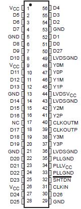
SN75LVDS81: Features: · 28:4 Data Channel Compression at up to 227.5 Million Bytes per Second Throughput· Suited for SVGA, XGA, or SXGA Display Data Transmission From Controller to Display With Very Low EMI· 28...
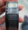
floor Price/Ceiling Price

Part Number:
SN75LVDS81
Supply Ability:
5000

Price Break

  • Qty
  • 1~5000
  • Unit Price
  • Negotiable
  • Processing time
  • 15 Days
Total Cost: $ 0.00

SeekIC Buyer Protection PLUS - newly updated for 2013!

  • Escrow Protection.
  • Guaranteed refunds.
  • Secure payments.
  • Learn more >>

Month Sales

268 Transactions

Rating

evaluate  (4.8 stars)

Upload time: 2025/12/24

Payment Methods

All payment methods are secure and covered by SeekIC Buyer Protection PLUS.

Notice: When you place an order, your payment is made to SeekIC and not to your seller. SeekIC only pays the seller after confirming you have received your order. We will also never share your payment details with your seller.
Product Details

Description


Features:

· 28:4 Data Channel Compression at up to 227.5 Million Bytes per Second Throughput
· Suited for SVGA, XGA, or SXGA Display Data Transmission From Controller to Display With Very Low EMI
· 28 Data Channels and Clock In Low-Voltage TTL
· 4 Data Channels and Clock-Out Low-Voltage Differential
· Operates From a Single 3.3-V Supply With 250 mW (Typ)
· 5-V Tolerant Data Inputs
· Falling Clock-Edge-Triggered Inputs
· Packaged in Thin Shrink Small-Outline Package With 20-Mil Terminal Pitch
· Consumes Less Than 1 mW When Disabled
· Wide Phase-Lock Input Frequency Range . . . 31 MHz to 68 MHz
· No External Components Required for PLL
· Outputs Meet or Exceed the Requirements of ANSI EIA/TIA-644 Standard
· Improved Replacement for the National DS90C581


Pinout

  Connection Diagram


Specifications

Supply voltage range, VCC (see Note 1) . . . . . . . . . . . . . . . . . . . . . . . . . . . . . . . . . . . . 0.3 V to 4 V
Output voltage range, VO (all terminals) . . . . . . . . . . . . . . . . . . . . . . . . . . . . . 0.3 V to VCC + 0.5 V
Input voltage range, VI (all terminals) . . . . . . . . . . . . . . . . . . . . . . . . . . . . . . . . . . . . 0.5 V to 5.5 V
Continuous total power dissipation . . . . . . . . . . . . . . . . . . . . . . . . . .. . . see Dissipation Rating Table
Storage temperature range, Tstg . . . . . . . . . . . . . . . . . . . . . . . . . . . . . .. . . . . . . . . . 65 to 150
Lead temperature 1,6 mm (1/16 inch) from case for 10 seconds . . . . . . . . . . . . . . . . . . .  . . . . .260

† Stresses beyond those listed under "absolute maximum ratings" may cause permanent damage to the device. These are stress ratings only, and functional operation of the device at these or any other conditions beyond those indicated under "recommended operating conditions" is not implied. Exposure to absolute-maximum-rated conditions for extended periods may affect device reliability.
NOTES: 1. All voltage values are with respect to the GND terminals.


Description

The SN75LVDS81 FlatLink transmitter contains four 7-bit parallel-load serial-out shift registers, a 7× clock synthesizer, and five low-voltage differential-signaling (LVDS) line drivers in a single integrated circuit. These functions allow 28 bits of single-ended LVTTL data to be synchronously transmitted over five balanced-pair conductors for receipt by a compatible receiver, such as the SN75LVDS82. The SN75LVDS81 can also be used in 21-bit links with the SN75LVDS86 receiver.

When SN75LVDS81 transmitting, data bits D0 through D27 are each loaded into registers upon the falling edge of the input clock signal (CLKIN) The frequency of CLKIN is multiplied seven times (7×) and then used to unload the data registers in 7-bit slices and serially. The four serial streams and a phase-locked clock (CLKOUT) are then output to LVDS output drivers. The frequency of CLKOUT is the same as the input clock, CLKIN.

The SN75LVDS81 requires no external components and little or no control. The data bus appears the same at the input to the transmitter and output of the receiver with the data transmission transparent to the user. The only user intervention is the possible use of the shutdown/clear (SHTDN) active-low input to inhibit the clock and shut off the LVDS output drivers for lower power consumption. A low-level on SHTDN clears all internal registers to a low level.

The SN75LVDS81 is characterized for operation over free-air temperature ranges of 0C to 70C.


Customers Who Bought This Item Also Bought

Margin,quality,low-cost products with low minimum orders. Secure your online payments with SeekIC Buyer Protection.
Inductors, Coils, Chokes
Boxes, Enclosures, Racks
Cable Assemblies
Hardware, Fasteners, Accessories
Undefined Category
View more