Features: · 3:21 Data Channel Expansion at up to 163 Million Bytes per Second Throughput
· Suited for SVGA, XGA, or SXGA Display Data Transmission From Controller to Display With Very Low EMI
· 3 Data Channels and Clock Low-Voltage Differential Channels In and 21 Data and Clock Low-Voltage TTL Channels Out
· Operates From a Single 3.3-V Supply and 250 mW (Typ)
· 5-V Tolerant SHTDN Input
· ESD Protection Exceeds 4 kV on Bus Pins
· Packaged in Thin Shrink Small-Outline Package (TSSOP) With 20-Mil Terminal Pitch
· Consumes Less Than 1 mW When Disabled
· Wide Phase-Lock Input Frequency Range 31 MHz to 68 MHz
· No External Components Required for PLL
· Open-Circuit Receiver Fail-Safe Design
· Inputs Meet or Exceed the Requirements of ANSI EIA/TIA-644 Standard
· Improved Replacement for the DS90C562Pinout Specifications
Supply voltage range, VCC (see Note 1) . . . . . . . . . . . . . . . . . . . . . . . . . . . . . . . . . . 0.5 V to 4 V
Output voltage range, VO (Dxx terminals) . . . . . . . . . . . . . . . . . . . . . . . .. . . 0.5 V to VCC + 0.5 V
Input voltage range, VI (any terminal except SHTDN) . . . . . . . . . . . . . . . . . .0.5 V to VCC + 0.5 V
Input voltage range, VI (SHTDN) . . . . . . . . . . . . . . . . . . . . . . . . . . . . . . . . . . . . . . 0.5 V to 5.5 V
Continuous total power dissipation . . . . . . . . . . . . . . . . . . . . . . . . . . See Dissipation Rating Table
Storage temperature range, Tstg . . . . . . . . . . . . . . . . . . . . . . . . . . . . . . . . .. . . . . 65 to 150
Lead temperature 1,6 mm (1/16 inch) from case for 10 seconds . . . . . . . . . . . . . . . . . .. . . . 260
† Stresses beyond those listed under "absolute maximum ratings" may cause permanent damage to the device. These are stress ratings only, and functional operation of the device at these or any other conditions beyond those indicated under "recommended operating conditions" is not implied. Exposure to absolute-maximum-rated conditions for extended periods may affect device reliability.
NOTES: 1. All voltage values are with respect to GND unless otherwise noted.
DescriptionThe SN75LVDS86 FlatLink receiver contains three serial-in 7-bit parallel-out shift registers, a 7* clock synthesizer, and four low-voltage differential signaling (LVDS) line receivers in a single integrated circuit. These functions allow receipt of synchronous data from a compatible transmitter, such as the SN75LVDS81, '83, '84, or '85, over four balanced-pair conductors and expansion to 21 bits of single-ended low-voltage TTL (LVTTL) synchronous data at a lower transfer rate.
When receiving, the high-speed LVDS data is received and loaded into registers at seven times the LVDS input clock (CLKIN) rate. The data is then unloaded to a 21-bit wide LVTTL parallel bus at the CLKIN rate. A phase-locked loop clock synthesizer circuit generates a 7* clock for internal clocking and an output clock for the expanded data. The SN75LVDS86 presents valid data on the falling edge of the output clock (CLKOUT).
The SN75LVDS86 requires only four line-termination resistors for the differential inputs and little or no control. The data bus appears the same at the input to the transmitter and output of the receiver with the data transmission transparent to the user(s). The only possible user intervention is the use of the shutdown/clear (SHTDN) active-low input to inhibit the clock and shut off the LVDS receivers for lower power consumption. A low level on this signal clears all internal registers to a low level.
The LVDS receivers of the SN75LVDS86 include an open-circuit fail-safe design such that when the inputs are not connected to an LVDS driver, the receiver outputs go to a low-level. This occurs even when the line is differentially terminated at the receiver inputs.
The SN75LVDS86 is characterized for operation over ambient free-air temperatures of 0�C to 70�C.

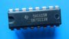
 SN75LVDS86 Data Sheet