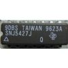
SNJ54CBT16209WD

Features: ·Members of the Texas Instruments WidebusTM Family·5-Ω Switch Connection Between Two Ports·TTL-Compatible Input LevelsPinoutSpecificationsSupply voltage range, VCC .............................................................−0.5 V to 7 V Input voltage range, VI (see Note 1) ...

product image

SNJ54CBT16209WD Picture
SeekIC No. : 004499963 Detail

SNJ54CBT16209WD: Features: ·Members of the Texas Instruments WidebusTM Family·5-Ω Switch Connection Between Two Ports·TTL-Compatible Input LevelsPinoutSpecificationsSupply voltage range, VCC .....................

floor Price/Ceiling Price

Part Number:
SNJ54CBT16209WD
Supply Ability:
5000

Price Break

  • Qty
  • 1~5000
  • Unit Price
  • Negotiable
  • Processing time
  • 15 Days
Total Cost: $ 0.00

SeekIC Buyer Protection PLUS - newly updated for 2013!

  • Escrow Protection.
  • Guaranteed refunds.
  • Secure payments.
  • Learn more >>

Month Sales

268 Transactions

Rating

evaluate  (4.8 stars)

Upload time: 2025/12/24

Payment Methods

All payment methods are secure and covered by SeekIC Buyer Protection PLUS.

Notice: When you place an order, your payment is made to SeekIC and not to your seller. SeekIC only pays the seller after confirming you have received your order. We will also never share your payment details with your seller.
Product Details

Description


Features:

·Members of the Texas Instruments  WidebusTM Family
·5-Ω Switch Connection Between Two Ports
·TTL-Compatible Input Levels


Pinout

  Connection Diagram


Specifications

Supply voltage range, VCC .............................................................−0.5 V to 7 V
Input voltage range, VI (see Note 1) .............................................−0.5 V to 7 V
Continuous channel current ....................................................................128 mA
Input clamp current, IIK (VI < 0)............................................................. −50 mA
Package thermal impedance, JA (see Note 2): DGG package ................70/W 
                                                                           DGV package ...............58/W 
                                                                           DL package .................63/W
Storage temperature range, Tstg ...............................................−65 to 150
† Stresses beyond those listed under "absolute maximum ratings" may cause permanent damage to the
   device. These are stress ratings only, and functional operation of the device at these or any other
   conditions  beyond those indicated under "recommended operating conditions" is not implied. Exposure
   to absolute-maximum-rated conditions for extended periods may affect device reliability.

NOTES: 1. The input and output negative-voltage ratings may be exceeded if the input and output clamp-
                 current ratings are observed.
            2. The package thermal impedance is calculated in accordance with JESD 51-7.


Description

The SNJ54CBT16209WD and SN74CBT16209A devices provide 18 bits of high-speed TTL-compatible bus switching or exchanging. The low on-state resistance of the switches allows connections to be made with minimal propagation delay.

The devices SNJ54CBT16209WD operate as an 18-bit bus switch or a 9-bit bus exchanger, which provides data exchanging between the four signal ports via the data-select (S0, S1, S2) terminals.


Customers Who Bought This Item Also Bought

Margin,quality,low-cost products with low minimum orders. Secure your online payments with SeekIC Buyer Protection.
Prototyping Products
DE1
Motors, Solenoids, Driver Boards/Modules
LED Products
Tapes, Adhesives
803
Cables, Wires
Resistors
View more