Features: ` Wide Operating Voltage Range of 2 V to 6 V` High-Current 3-State True Outputs Can Drive Up To 15 LSTTL Loads` Eight D-Type Flip-Flops in a Single Package` Full Parallel Access for Loading` Low Power Consumption, 80-A Max ICC` Typical tpd = 14 ns` ±6-mA Output Drive at 5 V` Low Input Cu...
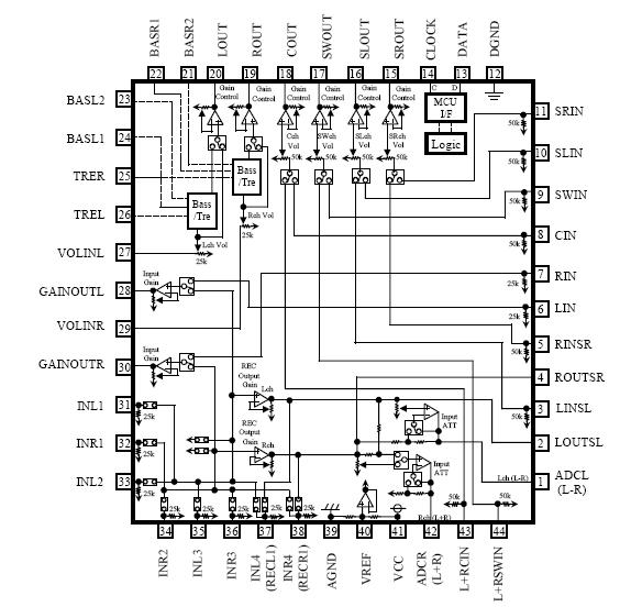
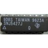
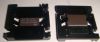
SNJ54HC374: Features: ` Wide Operating Voltage Range of 2 V to 6 V` High-Current 3-State True Outputs Can Drive Up To 15 LSTTL Loads` Eight D-Type Flip-Flops in a Single Package` Full Parallel Access for Loadin...
SeekIC Buyer Protection PLUS - newly updated for 2013!
268 Transactions
All payment methods are secure and covered by SeekIC Buyer Protection PLUS.
DescriptionThe SNJ54ABT827FK These 10-bit buffers or bus drivers provide a high-performance bus in...

Supply voltage range, VCC . . . . . . . . . . . . . . . . . . . . . . . . . . . . . . . . . . . . . . . . . . . . . . . . . . . . 0.5 V to 7 V
Input clamp current, IIK (VI < 0 or VI > VCC) (see Note 1) . . . . . . . . . . . . . . . . . . . . . . . . . . . . . . . . ±20 mA
Output clamp current, IOK (VO < 0 or VO > VCC) (see Note 1) . . . . . . . . . . . . . . . . . . . . . . . . . . . . . ±20 mA
Continuous output current, IO (VO = 0 to VCC) . . . . . . . . . . . . . . . . . . . . . . . . . . . . . . . . . . . . . . . . . ±35 mA
Continuous current through VCC or GND . . . . . . . . . . . . . . . . . . . . . . . . . . . . . . . . . . ... . . . . . . . . . . ±70 mA
Package thermal impedance, JA (see Note 2): DB package . . . . . . . . . . . . . . . . . . . . . . . . . . . . . . 70°C/W
DW package . . . . . . . . . . . . . . . . . . . . . . . . . . . . . . 58°C/W
N package . . . . . . . . . . . . . . . . . . . . . . . . . .. . . . . . . 69°C/W
NS package . . . . . . . . . . . . . . . . . . . . . . . . . . . . . .. . 60°C/W
PW package . . . . . . . . . . . . . . . . . . . . . . . .. . . . . .. . . 83°C/W
Storage temperature range, Tstg . . . . . . . . . . . . . . . . . . . . . . . . . . . . . . . . . . . . . . . . .. . . . . . 65°C to 150°C
† Stresses beyond those listed under "absolute maximum ratings" may cause permanent damage to the device. These are stress ratings only, and functional operation of the device at these or any other conditions beyond those indicated under "recommended operating conditions" is not implied. Exposure to absolute-maximum-rated conditions for extended periods may affect device reliability.
NOTES: 1. The input and output voltage ratings may be exceeded if the input and output current ratings are observed.
2. The package thermal impedance is calculated in accordance with JESD 51-7.
These 8-bit flip-flops feature 3-state outputs designed specifically for driving highly capacitive or relatively low-impedance loads. SNJ54HC374 are particularly suitable for implementing buffer registers, I/O ports, bidirectional bus drivers, and working registers.
The eight flip-flops of the SNJ54HC374 devices are edge-triggered D-type flip-flops. On the positive transition of the clock (CLK) input, the Q outputs are set to the logic levels that were set up at the data (D) inputs.An output-enable (OE) input places the eight outputs in either a normal logic state (high or low logic levels) or the high-impedance state. In the high-impedance state, the outputs neither load nor drive the bus lines significantly. The high-impedance state and increased drive provide the capability to drive bus lines without interface or pullup components.