SST27VF040

Features: • 2.7 to 3.6 Volt Read Operation• Superior Reliability Endurance: Greater than 1000 Cycles Greater than 100 years Data Retention• Low Power Consumption Active Current: 10 mA (typical) Standby Current: 10 A (typical)• Fast Access Time 90 and 120 ns• Fast...

product image

SST27VF040 Picture
SeekIC No. : 004505212 Detail

SST27VF040: Features: • 2.7 to 3.6 Volt Read Operation• Superior Reliability Endurance: Greater than 1000 Cycles Greater than 100 years Data Retention• Low Power Consumption Active Current:...

floor Price/Ceiling Price

Part Number:
SST27VF040
Supply Ability:
5000

Price Break

  • Qty
  • 1~5000
  • Unit Price
  • Negotiable
  • Processing time
  • 15 Days
Total Cost: $ 0.00

SeekIC Buyer Protection PLUS - newly updated for 2013!

  • Escrow Protection.
  • Guaranteed refunds.
  • Secure payments.
  • Learn more >>

Month Sales

268 Transactions

Rating

evaluate  (4.8 stars)

Upload time: 2025/12/24

Payment Methods

All payment methods are secure and covered by SeekIC Buyer Protection PLUS.

Notice: When you place an order, your payment is made to SeekIC and not to your seller. SeekIC only pays the seller after confirming you have received your order. We will also never share your payment details with your seller.
Product Details

Description


Features:

• 2.7 to 3.6 Volt Read Operation
• Superior Reliability
  Endurance: Greater than 1000 Cycles
  Greater than 100 years Data Retention
• Low Power Consumption
  Active Current: 10 mA (typical)
  Standby Current: 10 A (typical)
• Fast Access Time
  90 and 120 ns
• Fast Programming Operation
  10s Programming Pulse
  Chip Programming Time of 7 seconds
• Features Electrical Erase
  Does Not Require UV Source
  Chip Erase Time: 100 ms
• CMOS I/O Compatibility
• JEDEC Standard Byte-wide EPROM Pinouts
• 12V Power Supply for Programming/Erase
• Packages Available
  32-Pin PLCC
  32-Pin Plastic DIP
  32-Pin TSOP (8mm x 14mm)


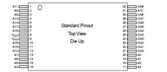
Pinout

  Connection Diagram


Specifications

Applied conditions greater than those listed under "Absolute Maximum Stress Ratings" may cause
permanent damage to the device. This is a stress rating only and functional operation of the device
at these conditions or conditions greater than those defined in the operational sections of this data
sheet is not implied.Exposure to absolute maximum stress rating conditions may affect device reliability.

Temperature Under Bias .......................................................................................   ............. -55 to +125
Storage Temperature ........................................................................................................... -65 to +150
D. C. Voltage on Any Pin to Ground Potential ................................................................. -0.5V to VDD+ 0.5V
Transient Voltage (<20 ns) on Any Pin to Ground Potential ........................................... -1.0V to VDD+ 1.0V
Voltage on A9, and VPP Pin to Ground Potential .............................................................. ..... -0.5V to 13.2V
Package Power Dissipation Capability (TA = 25) ............................................................................... 1.0W
Through Hole Lead Soldering Temperature (10 Seconds) ....................................................................300
Surface Mount Lead Soldering Temperature (3 Seconds) ............................................................. ...... 240
Output Short Circuit Current(1) ................................................................................................... ...... 50 mA


Description

The SST27VF040 is a 512K x 8 CMOS, many-time programmable (MTP) low cost flash, manufactured with SST's proprietary, high performance CMOS SuperFlash technology. The split gate cell design and thick oxide tunneling injector attain better reliability and manufacturability compared with alternate approaches.The SST27VF040 can be electrically erased and programmed at least 1000 times using an external programmer,e.g., to change the contents of devices in inventory.The SST27VF040 has to be erased prior to programming.The SST27VF040 conforms to JEDEC standard pinouts for byte-wide memories.

Featuring high performance byte programming, the SST27VF040 uses a programming pulse of 10 s. The entire memory can be programmed byte by byte in 7 seconds. Designed, manufactured, and tested for a wide spectrum of applications, the SST27VF040 is offered with a endurance of 1000 cycles. Data retention is rated at greater than 100 years.

The SST27VF040 is suited for applications that require infrequent writes and low power nonvolatile storage. The SST27VF040 will improve flexibility, efficiency, and performance while matching the low cost in nonvolatile applications that currently use UV-EPROMs, OTPs, and
mask ROMs.

To meet surface mount and conventional through hole requirements, the SST27VF040 is offered in 32-pin PLCC, 32-pin PDIP and 32-pin TSOP packages. See Figures 1 and 2 for pinouts


Customers Who Bought This Item Also Bought

Margin,quality,low-cost products with low minimum orders. Secure your online payments with SeekIC Buyer Protection.
Sensors, Transducers
Cable Assemblies
Motors, Solenoids, Driver Boards/Modules
Cables, Wires
Test Equipment
View more