SeekIC No. : 004505216
Detail
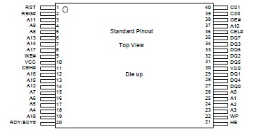
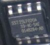
SST28LP040: Features: Single 3.0-Volt Read and Write Operations CMOS SuperFlash EEPROM Technology -Endurance: 250,000 Cycles (typical) -Greater than 100 years Data RetentionMemory Organization: -512K x 8/1M x 4...
 SST28LP040 Data Sheet
floor Price/Ceiling Price
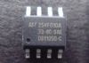
- Part Number:
- SST28LP040
- Supply Ability:
- 5000
Price Break
- Qty
- 1~5000
- Unit Price
- Negotiable
- Processing time
- 15 Days
SeekIC Buyer Protection PLUS - newly updated for 2013!
- Escrow Protection.
- Guaranteed refunds.
- Secure payments.
- Learn more >>
Month Sales
268 Transactions
Payment Methods
All payment methods are secure and covered by SeekIC Buyer Protection PLUS.
Notice: When you place an order, your payment is made to SeekIC and not to your seller. SeekIC only pays the seller after confirming you have received your order. We will also never share your payment details with your seller.