SST31LH021

Features: • Organized as 256K x 8 flash + 128K x 8 SRAM• Single 3.0-3.6V Read and Write Operations• Concurrent Operation Read from or write to SRAM while erase/program Flash• Superior Reliability Endurance: 100,000 Cycles (typical) Greater than 100 years Data Retention&#...

product image

SST31LH021 Picture
SeekIC No. : 004505254 Detail

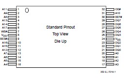
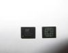
SST31LH021: Features: • Organized as 256K x 8 flash + 128K x 8 SRAM• Single 3.0-3.6V Read and Write Operations• Concurrent Operation Read from or write to SRAM while erase/program Flash•...

floor Price/Ceiling Price

Part Number:
SST31LH021
Supply Ability:
5000

Price Break

  • Qty
  • 1~5000
  • Unit Price
  • Negotiable
  • Processing time
  • 15 Days
Total Cost: $ 0.00

SeekIC Buyer Protection PLUS - newly updated for 2013!

  • Escrow Protection.
  • Guaranteed refunds.
  • Secure payments.
  • Learn more >>

Month Sales

268 Transactions

Rating

evaluate  (4.8 stars)

Upload time: 2025/12/23

Payment Methods

All payment methods are secure and covered by SeekIC Buyer Protection PLUS.

Notice: When you place an order, your payment is made to SeekIC and not to your seller. SeekIC only pays the seller after confirming you have received your order. We will also never share your payment details with your seller.
Product Details

Description


Features:

• Organized as 256K x 8 flash + 128K x 8 SRAM
• Single 3.0-3.6V Read and Write Operations
• Concurrent Operation
  Read from or write to SRAM while erase/program Flash
• Superior Reliability
  Endurance: 100,000 Cycles (typical)
  Greater than 100 years Data Retention
• Low Power Consumption:
  Active Current: 10 mA (typical) for Flash or SRAM Read
  Standby Current: 10 A (typical)
• Sector Erase Capability
  Uniform 4 KByte sectors
• Fast Read Access Times:
  Flash: 70 ns
  SRAM: 25 ns
• Latched Address and Data for Flash
• Flash Fast Sector Erase and Byte Program:
  Sector Erase Time: 18 ms typical
  Bank Erase Time: 70 ms typical
  Byte Program Time: 14 s typical
  Bank Rewrite Time: 4 seconds typical
• Flash Automatic Erase and Program Timing
  Internal VPP Generation
• Flash End of Write Detection
  Toggle Bit
  Data# Polling
• CMOS I/O Compatibility
• JEDEC Standard Command Set
• Packages Available
  32-Pin TSOP (8mm x 14mm)
  40-Pin TSOP (10mm x 14mm


Pinout

  Connection Diagram


Specifications

Temperature Under Bias ......................................................................................... -55 to +125
Storage Temperature ............................................................................................. -65 to +150
D. C. Voltage on Any Pin to Ground Potential ....................................................-0.5V to VDD+ 0.5V
Transient Voltage (<20 ns) on Any Pin to Ground Potential ............................. -1.0V to VDD+ 1.0V
Voltage on A9 Pin to Ground Potential ..................................................................... -0.5V to 13.2V
Package Power Dissipation Capability (Ta = 25) ................................................................. 1.0W
Surface Mount Lead Soldering Temperature (3 Seconds) ...................................................... 240
Output Short Circuit Curre(1) ............................................................................................... 50 mA


Description

The SST31LH021 is a 256K x 8 CMOS flash memory bank combined with a 128K x 8 CMOS SRAM memory bank manufactured with SST's proprietary, high performance SuperFlash technology. The SST31LH021 device writes (SRAM or programs or erases flash) with a 3.0-3.6V power supply. The monolithic SST31LH021 device conforms to JEDEC standard pinouts and Software Data Protect (SDP) commands for x8 EEPROMs in TSOP packages.


Customers Who Bought This Item Also Bought

Margin,quality,low-cost products with low minimum orders. Secure your online payments with SeekIC Buyer Protection.
Hardware, Fasteners, Accessories
Memory Cards, Modules
Sensors, Transducers
Batteries, Chargers, Holders
View more