Features: • Organized as 128K x16 / 256K x16 / 512K x16
• Single Voltage Read and Write Operations
3.0-3.6V for SST39LF200A/400A/800A
2.7-3.6V for SST39VF200A/400A/800A
• Superior Reliability
Endurance: 100,000 Cycles (typical)
Greater than 100 years Data Retention
• Low Power Consumption
Active Current: 20 mA (typical)
Standby Current: 3 µA (typical)
• Sector-Erase Capability
Uniform 2 KWord sectors
• Block-Erase Capability
Uniform 32 KWord blocks
• Fast Read Access Time
45 and 55 ns for SST39LF200A/400A
55 ns for SST39LF800A
70 and 90 ns for SST39VF200A/400A/800A
• Latched Address and Data
• Fast Erase and Word-Program
Sector-Erase Time: 18 ms (typical)
Block-Erase Time: 18 ms (typical)
Chip-Erase Time: 70 ms (typical)
Word-Program Time: 14 µs (typical)
Chip Rewrite Time:
2 seconds (typical) for SST39LF/VF200A
4 seconds (typical) for SST39LF/VF400A
8 seconds (typical) for SST39LF/VF800A
• Automatic Write Timing
Internal VPP Generation
• End-of-Write Detection
Toggle Bit
Data# Polling
• CMOS I/O Compatibility
• JEDEC Standard
Flash EEPROM Pinouts and command sets
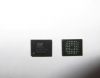
• Packages Available
48-lead TSOP (12mm x 20mm)
48-ball TFBGA (6mm x 8mm)Pinout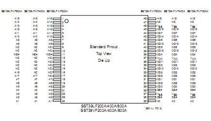
SpecificationsTemperature Under Bias . . . . . . . . . . . . . . . . . . . . . . . . . . . . . . . . . .. . -55°C to +125°C
Storage Temperature . . . . . . . . . . . . . . . . . . . . . . . . . . .. . . . . . . . . . . -65°C to +150°C
D. C. Voltage on Any Pin to Ground Potential . . . .. . . .. . . . . . . . . . .. . -0.5V to VDD + 0.5V
Transient Voltage (<20 ns) on Any Pin to Ground Potential . . . . . .. . -1.0V to VDD + 1.0V
Voltage on A9 Pin to Ground Potential . . . . . . . . . . . . . . . . . . . . . . . . . . . . . -0.5V to13.2V
Package Power Dissipation Capability (Ta = 25°C) . . . . . . . . . . . . . . . . . . . . . . . . . . 1.0W
Surface Mount Lead Soldering Temperature (3 Seconds) . . . . . . . . . . . . .. .. . . . . 240°C
Output Short Circuit Current1 . . . . . . . . . . . . . . . . . . . . . . . . . . . . . . . . . . . . . . 50 mA
DescriptionThe SST39LF200A/400A/800A and SST39VF200A/400A/800A devices are suited for applications that require conve-nient and economical updating of program, configuration, or data memory. For all system applications, they signifi cantly improve performance and reliability, while lowering power consumption. They inherently use less energy dur- ing Erase and Program than alternative flash technologies. When programming a flash device, the total energy consumed is a function of the applied voltage, current, and time of application. Since for any given voltage range, the SuperFlash technology uses less current to program and has a shorter erase time, the total energy consumed during any Erase or Program operation is less than alternative flash technologies. These devices also improve flexibility while lowering the cost for program, data, and configuration storage applications.
The SuperFlash technology provides fixed Erase and Pro-gram times, independent of the number of Erase/Program cycles that have occurred. Therefore the system software or hardware does not have to be modified or de-rated as is necessary with alternative flash technologies, whose Erase and Program times increase with accumulated Erase/Program cycles.
To meet surface mount requirements, the SST39LF200A/400A/800A and SST39VF200A/400A/800A are offered in both 48-lead TSOP packages and 48-ball TFBGA pack-ages. See Figures 1 and 2 for pinouts.

 SST39VF200A Data Sheet