Features: * Firmware Hub for Intel 8xx Chipsets
* 2 Mbit, 3 Mbit, 4 Mbit, or 8 Mbit SuperFlash memory array for code/data storage
SST49LF002A: 256K x8 (2 Mbit)
SST49LF003A: 384K x8 (3 Mbit)
SST49LF004A: 512K x8 (4 Mbit)
SST49LF008A: 1024K x8 (8 Mbit)
* Flexible Erase Capability
Uniform 4 KByte Sectors
Uniform 16 KByte overlay blocks for
SST49LF002A
Uniform 64 KByte overlay blocks for
SST49LF003A/004A/008A
Top Boot Block protection
- 16 KByte for SST49LF002A
- 64 KByte for SST49LF003A/004A/008A
Chip-Erase for PP Mode Only
* Single 3.0-3.6V Read and Write Operations
* Superior Reliability
Endurance:100,000 Cycles (typical)
Greater than 100 years Data Retention
* Low Power Consumption
Active Read Current: 6 mA (typical)
Standby Current: 10 A (typical)
* Fast Sector-Erase/Byte-Program Operation
Sector-Erase Time: 18 ms (typical)
Block-Erase Time: 18 ms (typical)
Chip-Erase Time: 70 ms (typical)
Byte-Program Time: 14 s (typical)
Chip Rewrite Time:
SST49LF002A: 4 seconds (typical)
SST49LF003A: 6 seconds (typical)
SST49LF004A: 8 seconds (typical)
SST49LF008A: 15 seconds (typical)
Single-pulse Program or Erase
Internal timing generation
* Two Operational Modes
Firmware Hub Interface (FWH) Mode for in-system operation
Parallel Programming (PP) Mode for fast production programming
* Firmware Hub Hardware Interface Mode
5-signal communication interface supporting byte Read and Write
33 MHz clock frequency operation
WP# and TBL# pins provide hardware write protect for entire chip and/or top Boot Block
Block Locking Register for all blocks
Standard SDP Command Set
Data# Polling and Toggle Bit for End-of-Write detection
5 GPI pins for system design flexibility
4 ID pins for multi-chip selection
* Parallel Programming (PP) Mode
11-pin multiplexed address and 8-pin data I/O interface
Supports fast In-System or PROM programming for manufacturing
* CMOS and PCI I/O Compatibility
* Packages Available
32-lead PLCC
32-lead TSOP (8mm x 14mm)Pinout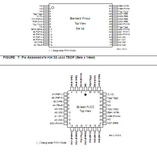 SpecificationsTemperature Under Bias . . . . . . . . . . . . . . . . . . . . . . . . . . . . . . . . .. -55 to +125
Storage Temperature. . . . . . . . . . . . . . . . . . . . . . . . . . . . . . . . . . . ..-65 to +150
D. C. Voltage on Any Pin to Ground Potential . . . . . . . . . . . . . . . -0.5V to VDD +0.5V
Transient Voltage (<20 ns) on Any Pin to Ground Potential1. . . -2.0V to VDD +2.0V
Package Power Dissipation Capability (Ta=25!aC) . . . . . . . . . . . . . . . . . . . . . 1.0W
Surface Mount Lead Soldering Temperature (3 Seconds). . . . . . . . . . . . . . . 240
Output Short Circuit Current2. . . . . . . . . . . . . . . . . . . . . . . . . . . . . . . . . . . .. 50 mA
1.Do not violate processor or chipset limitations on the INIT# pin.
2.Outputs shorted for no more than one second. No more than one output shorted at a time. This note applies to non-PCI outputs. DescriptionThe SST49LF003A flash memory devices are manufac-tured with SST!s proprietary, high performance Super Flash Technology. The split-gate cell design and thick oxide tunneling injector attain better reliability and manu-facturability compared with alternate approaches. The SST49LF00xA devices significantly improve performance and reliability, while lowering power consumption. The SST49LF00xA devices write (Program or Erase) with a single 3.0-3.6V power supply. It uses less energy during Erase and Program than alternative flash memory tech- nologies. The total energy consumed is a function of the applied voltage, current and time of application. Since for any given voltage range, the SuperFlash technology uses less current to program and has a shorter erase time, the total energy consumed during any Erase or Program oper- ation is less than alternative flash memory technologies.The SST49LF00xA products provide a maximum Byte- Program time of 20 |ìsec. The entire memory can be erased and programmed byte-by-byte typically in 15 sec-onds for an 8-Mbit device, when using status detection features such as Toggle Bit or Data# Polling to indicate the completion of Program operation. The SuperFlash tech-nology provides fixed Erase and Program time, indepen-dent of the number of Erase/Program cycles that have performed. Therefore the system software or hardware does not have to be calibrated or correlated to the cumu- lated number of Erase/Program cycles as is necessary with alternative flash memory technologies, whose Erase and Program time increase with accumulated Erase/Pro- gram cycles.
To protect against inadvertent write, the SST49LF003A devices employ hardware and software data (SDP) protec-tion schemes. It is offered with typical endurance of 100,000 cycles. Data retention is rated at greater than 100
years.
To meet high density, surface mount requirements,the SST49LF003A device is offered in 32-lead TSOP and 32-lead PLCC packages. See Figures 7 and 8 for pinouts and Table 8 for pin descriptions.

 SST49LF003A Data Sheet