Features: • Organized as 2M x8
• Conforms to Intel® LPC Interface Specification v1.1
Support Multi-Byte Firmware Memory Read/ Write Cycles
• Single 3.0-3.6V Read and Write Operations
• LPC Mode
5-signal LPC bus interface for both in-system and factory programming using programmer equipment
Multi-Byte Read capability allowing 15.6 MB/s data transfer rate @ 33 MHz PCI clock
- Firmware Memory Read cycle supporting 1, 2, 4, 16, and 128 Byte Read
- Firmware Memory Write cycle supporting 1, 2, and 4 Byte Write
33 MHz clock frequency operation
WP#/AAI and TBL# pins provide hardware Write protect for entire chip and/or top Boot Block
Block Locking Registers for individual block Read- Lock, Write-Lock, and Lock-Down protection
5 GPI pins for system design flexibility
4 ID pins for multi-chip selection
Multi-Byte capability registers (read-only registers)
Status register for End-of-Write detection
Program-/Erase-Suspend Read or Write to other blocks during Program-/Erase-Suspend
• Two-cycle Command Set
• Security ID Feature
256-bit Secure ID space
- 64-bit Unique Factory Pre-programmed Device Identifier
- 192-bit User-Programmable OTP
• Superior Reliability
Endurance: 100,000 Cycles (typical)
Greater than 100 years Data Retention
• Low Power Consumption
Active Read Current: 12 mA (typical)
Standby Current: 10 A (typical)
• Uniform 4 KByte sectors
35 Overlay Blocks: one 16-KByte Boot Block, two 8-KByte Parameter Blocks, one 32-Kbyte Parameter Block, thirty-one 64-KByte Main Blocks.
• Fast Sector-Erase/Program Operation
Sector-Erase Time: 18 ms (typical)
Block-Erase Time: 18 ms (typical)
Program Time: 7 s (typical)
• Auto Address Increment (AAI) for Rapid Factory Programming (High Voltage Enabled)
RY/BY# pin for End-of-Write detection
Multi-Byte Program
Chip Rewrite Time: 4 seconds (typical)
• Packages Available
32-lead PLCC
32-lead TSOP (8mm x 14mm)
• All non-Pb (lead-free) devices are RoHS compliantPinout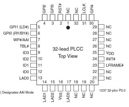 Specifications
Temperature Under Bias . . . . . . . . . . . . . . . . . . . . . . . . . . . . . . . . . . . . . . . . . . . . . . . -55°C to +125°C
Storage Temperature . . . . . . . . . . . . . . . . . . . . . . . . . . . . . . . . . . . . . . . . . . . . . . . . . -65°C to +150°C
D.C. Voltage on Any Pin to Ground Potential . . . . . . . . . . . . . . . . . . . . . . . . . . . . . . . . -0.5V to VDD+0.5V
Transient Voltage (<20 ns) on Any Pin (except WP#/AAI) to Ground Potential1 . . . . . . . -2.0V to VDD+2.0V
Voltage on WP#/AAI Pin to Ground Potential2. . . . . . . . . . . . . . . . . . . . . . . . . . . . . . . . . . .. -0.5V to 11.0V
Package Power Dissipation Capability (TA=25°C) . . . . . . . . . . . . . . . . . . . . . . . . . . . . . . . . . . . . . . . .1.0W
Surface Mount Solder Reflow Temperature3 . . . . . . . . . . . . . . . . . . . . . . . . . . . . . . .260°C for 10 seconds
1. Do not violate processor or chipset specification regarding INIT# voltage.
2. The maximum DC voltage on WP#/AAI pin may reach 11V for periods <20ns.
3. Excluding certain with-Pb 32-PLCC units, all packages are 260°C capable in both non-Pb and with-Pb solder versions.
Certain with-Pb 32-PLCC package types are capable of 240°C for 10 seconds; please consult the factory for the latest information.
4. Outputs shorted for no more than one second. No more than one output shorted at a time.
DescriptionThe SST49LF016C flash memory device is designed to interface with host controllers (chipsets) that support a lowpin- count (LPC) interface for system firmware applications. The SST49LF016C device complies with Intel's LPC Interface Specification 1.1, supporting a Burst-Read (up to 128 bytes in a single operation) which enables a 15.6 MByte per second data transfer. The LPC interface operates with 5 signal pins versus 28 pins of a 8-bit parallel flash memory. This frees up pins on the ASIC host controller resulting in lower ASIC costs and a reduction in overall system costs due to simplified signal routing.
The SST49LF016C uses a 5-signal LPC interface to support both in-system and rapid factory programming using programmer equipment. A high voltage pin (WP#/AAI) is used to enable Auto Address Increment (AAI) mode. The SST49LF016C offers hardware block protection in addition to individual block protection via software registers for critical system code and data. A 256-bit Security ID space with a 64-bit factory pre-programmed unique number and a 192- bit user programmable OTP area enhances the user's ability to use new security techniques and implement a new data protection scheme. The SST49LF016C also provides general purpose inputs (GPI) for system design flexibility. The SST49LF016C flash memory device is manufactured with SST's proprietary, high-performance SuperFlash technology.
The split-gate cell design and thick-oxide tunneling injector attain greater reliability and manufacturability compared with alternative technology approaches. The SST49LF016C device significantly improves performance and reliability, while lowering power consumption. The SST49LF016C device writes (Program or Erase) in-system with a single 3.0-3.6V power supply. It uses less energy during Erase and Program than alternative flash memory technologies.
The total energy consumed is a function of the applied voltage, current and time of application. Since for any given voltage range, the SuperFlash technology uses less current to program and has a shorter erase time, the total energy consumed during any Erase or Program operation is less than alternative flash memory technologies.
The SuperFlash technology provides fixed Erase and Program time, independent of the number of Erase/Program cycles that have performed. Therefore the system software or hardware does not have to be calibrated or correlated to the cumulative number of erase cycles as is necessary with alternative flash memory technologies, whose Erase and Program time increase with accumulated Erase/Program cycles. To protect against inadvertent write, the ST49LF016C device has on-chip hardware and software write protection schemes. It is offered with a typical endurance of 100,000 cycles. Data retention is rated at greater than 100 years.
The SST49LF016C product provides a maximum program time of 10 s per byte with a single-byte Program operation; effectively 5 s per byte with a dual-byte Program operation and 2.5 s per byte with a quad-byte Program operation. End-of-Write can be detected by the RY/BY# pin output in AAI mode and by reading the software status register during an in-system Program or Erase operation.
The SST49LF016C is offered in 32-PLCC and 32-TSOP packages. In addition, the SST49LF016C devices are offered in lead-free (non-Pb) package options to address the growing need for non-Pb solutions in electronic components. Non-Pb package versions can be obtained by ordering products with a package code suffix of "E" as the environmental attribute in the product part number. See Figures 2 and 3 for pin assignments and Table 1 for pin descriptions.

 SST49LF016C Data Sheet