Features: • Stub-series terminated logic for 2.5 V VDD (SSTL_2)
• Designed for PC1600PC2700 (at 2.5 V) and PC3200 (at 2.6 V) applications
• Pin and function compatible with JEDEC standard SSTV16859
• Supports SSTL_2 signal inputs as per JESD 89
• Flow-through architecture optimizes PCB layout
• ESD classification testing is done to JEDEC Standard JESD22.Protection exceeds 2000 V to HBM per method A114.
• Latch-up testing is done to JEDEC Standard JESD78, which exceeds 100 mA.
• Supports efficient low power standby operation
• Full DDR solution when used with PCKVF857
• Available in 56-terminal HVQFN packagesPinout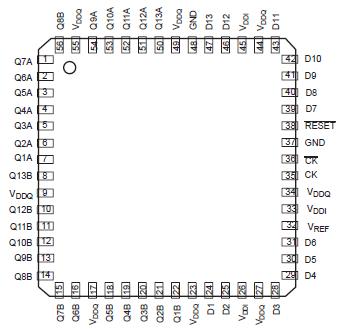 Specifications
|
SYMBOL |
PARAMETER |
CONDITION |
LIMITS |
UNIT |
|
Min |
Max |
|
VDD |
Supply voltage range |
|
0.5 |
+3.6 |
V |
|
VI |
Input voltage range |
Notes 2 and 3 |
0.5 |
VDD + 0.5 |
V |
|
VO |
Output voltage range |
Notes 2 and 3 |
0.5 |
VDD + 0.5 |
V |
|
IIK |
Input clamp current |
VI< 0 V or VI >VDD |
- |
±50 |
mA |
|
IOK |
Output clamp current |
VO< 0 V or VO >VDD |
- |
±50 |
mA |
|
IO |
Continuous output current |
VO = 0 V to VDD |
- |
±50 |
mA |
| |
Continuous current through each
VDD or GND |
|
- |
±100 |
mA |
|
Tstg |
Storage temperature range |
|
65 |
+150 |
|
DescriptionThe SSTVN16859 is a 13-bit to 26-bit SSTL_2 registered driver with differential clock inputs, designed to operate between 2.3 V and 2.7 V for PC1600 -PC2700 applications or between 2.5 V and 2.7 V for PC3200 applications. All inputs are compatible with the JEDEC standard for SSTL_2 with VREF normally at 0.5*VDD, except the LVCMOS reset (RESET) input. All outputs are SSTL_2, Class II compatible which can be used for standard stub-series applications or capacitive loads. Master reset (RESET) asynchronously resets all registers to zero.The SSTVN16859 is intended to be incorporated into standard DIMM (Dual In-Line Memory Module) designs defined by JEDEC,such as DDR (Double Data Rate) SDRAM and SDRAM II Memory Modules. Different from traditional SDRAM, DDR SDRAM transfers data on both clock edges (rising and falling), thus doubling the peak bus bandwidth. A DDR DRAM rated at 133 MHz will have a burst rate of 266 MHz.
The SSTVN16859 data inputs consist of different receivers. One differential input is tied to the input pin while the other is tied to a reference input pad, which is shared by all inputs.
The clock input is fully differential (CK and CK) to be compatible with DRAM devices that are installed on the DIMM. Data are registered at the crossing of CK going HIGH, and CK going LOW. However,since the control inputs to the SDRAM change at only half the data rate, the device must only change state on the positive transition of the CK signal. In order to be able to provide defined outputs from the device even before a stable clock has been supplied, the device has an asynchronous input pin (RESET), which when held to the LOW state, resets all registers and all outputs to the LOW state.
The SSTVN16859 supports low-power standby operation. When RESET is LOW, the differential input receivers are disabled, and undriven (floating) data, clock, and reference voltage (VREF) inputs are allowed. In addition, when RESET is LOW, all registers are reset,and all outputs are forced LOW. The LVCMOS RESET input must always be held at a valid logic HIGH or LOW level.
To ensure defined outputs from the register before a stable clock has been supplied, RESET must be held in the LOW state during power-up.
In the DDR DIMM application,RESET is specified to be completely asynchronous with respect to CK and CK. Therefore, no timing relationship can be guaranteed between the two. When entering RESET, the register will be cleared and the outputs will be driven LOW. As long as the data inputs are LOW, and the clock is stable during the time from the LOW-to-HIGH transition of RESET until the input receivers are fully enabled, the SSTVN16859 outputs will remain LOW.

 SSTVN16859 Data Sheet