Features: The ST10F166 is the FLASH memory members of the ST10 family of microcontroller developed and produced by SGS-THOMSON Microelectronics in CMOS technology. they combine high CPU performance (up to 10 million instructions per second) with high peripheral functionality, enhanced IO-capabilit...
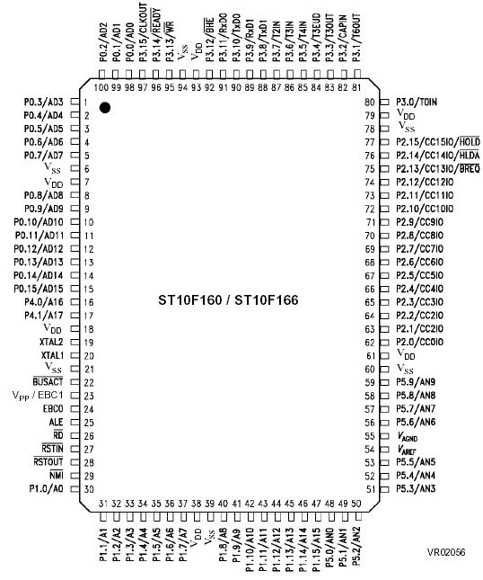
ST10F166: Features: The ST10F166 is the FLASH memory members of the ST10 family of microcontroller developed and produced by SGS-THOMSON Microelectronics in CMOS technology. they combine high CPU performance ...
SeekIC Buyer Protection PLUS - newly updated for 2013!
268 Transactions
All payment methods are secure and covered by SeekIC Buyer Protection PLUS.
Features: SpecificationsDescription This is the description of ST10 family: This programming manu...
The ST10F166 is the FLASH memory members of the ST10 family of microcontroller developed and produced by SGS-THOMSON Microelectronics in CMOS technology. they combine high CPU performance (up to 10 million instructions per second) with high peripheral functionality, enhanced IO-capabilities and an on-chip reprogrammable 32 KByte Flash Memory.
The ST10F166-16 derives its CPU clock signal (operating clock) directly from the onchip oscillator without using a prescaler.
With a clock duty cycle of 0.4 to 0.6, the recommended clock frequency is 16MHz for the ST10F166.
The ST10F166 operates at half the oscillator clock frequency (using a 2:1 oscillator prescaler).

Ambient temperature under bias (TA): . . . . . . . . . . . . . . . . . . . . .. . . 0 to +70 °C
Storage temperature (TST) . . . . . . . . . . . . . . . . . . . . . . . . . . . . 65 to +125 °C
Voltage on VCC pins with respect to ground (VSS). . . . . . . . . . . . .. 0.5 to +6.5 V
Voltage on any pin with respect to ground (VSS) . . . . . . . . . .. 0.3 to VCC +0.3 V
Input current on any pin during overload condition . . . . . . . . . . . .. -10 to +10 mA.
Absolute sum of all input currents during overload condition . . . . . . . . . . .100 mA.
Power dissipation . . . . . . . . . . . . . . . . . . . . . . . . . . . . . . . . . . . . . . . . . . . . . 1.5 W
Flash programming voltage (VPP). . . . . . . . . . . . . . . . . . . . . . . . 0.3 to + 13.5 V
Note: Stresses above those listed under "Absolute Maximum Ratings" may cause permanent damage to the device. This is a stress rating only and functional operation of the device at these or any other conditions above those indicated in the operational sections of this specification is not implied. Exposure to absolute maximum rating conditions for extended periods may affect device reliability. During overload conditions (VIN>VCC or VIN<VSS) the voltage on pins with respect to ground (VSS) must not exceed the values defined by the Absolute Maximum Ratings.