ST20-GP1

Features: · Application specific features· 12 channel GPS correlation DSP hardware and ST20 CPU (for control and position calu- culations) on one chip· no TCXO required· RTCA-SC159 / WAAS / EGNOS supported GPS performance· accuracy- stand alone with SA on <100m, SA off <30m- differential <...

product image

ST20-GP1 Picture
SeekIC No. : 004506355 Detail

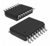
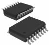
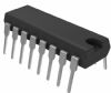
ST20-GP1: Features: · Application specific features· 12 channel GPS correlation DSP hardware and ST20 CPU (for control and position calu- culations) on one chip· no TCXO required· RTCA-SC159 / WAAS / EGNOS su...

floor Price/Ceiling Price

Part Number:
ST20-GP1
Supply Ability:
5000

Price Break

  • Qty
  • 1~5000
  • Unit Price
  • Negotiable
  • Processing time
  • 15 Days
Total Cost: $ 0.00

SeekIC Buyer Protection PLUS - newly updated for 2013!

  • Escrow Protection.
  • Guaranteed refunds.
  • Secure payments.
  • Learn more >>

Month Sales

268 Transactions

Rating

evaluate  (4.8 stars)

Upload time: 2025/12/23

Payment Methods

All payment methods are secure and covered by SeekIC Buyer Protection PLUS.

Notice: When you place an order, your payment is made to SeekIC and not to your seller. SeekIC only pays the seller after confirming you have received your order. We will also never share your payment details with your seller.
Product Details

Description


Features:

· Application specific features
· 12 channel GPS correlation DSP hardware and ST20 CPU (for control and position calu- culations) on one chip
· no TCXO required
· RTCA-SC159 / WAAS / EGNOS  supported GPS performance
· accuracy
- stand alone   with SA on <100m, SA off <30m
- differential <1m
- surveying <1cm
· time to first fix
- autonomous start 90s
- cold start 45s
- warm start 7s
- obscuration 1s 32-bit ST20 CPU
· 16/33 MHz processor clock
· 25 MIPS at 33 MHz
· fast integer/bit operations 4 Kbytes on-chip SRAM
· 130 Mbytes/s maximum bandwidth Programmable memory interface
· 4 separately configurable regions
· 8/16-bits wide
· support for mixed memory
· 2 cycle external access Serial communications
· Programmable UART (ASC)
· OS-Link Vectored interrupt subsystem
· 2 dedicated interrupt pins
· 5 levels of interrupt Power management
· low power operation
· power down modes Professional toolset support
· ANSI C compiler and libraries
· INQUEST advanced debugging tools Technology
· Static clocked 50 MHz design
· 3.3 V, sub micron technology 100 pin PQFP package


Application

· Global Positioning System (GPS) receivers
·Car navigation systems
·Fleet management systems
·Time reference for telecom systems


Description

The following section describes the functions of the EMI pins. Note that a signal name prexed by not indicates active low.

MemAddr1-19
External address bus. The ST20-GP1 uses 30 bits of addressing internally but only the bottom 18 bits are brought out to external pins (MemAddr2-19); MemAddr1 is generated by the EMI. MemAddr1-19 is valid and constant for the whole duration of an external access. The memory locations in each bank can be accessed at multiple addresses, as bits 20-29 are ignored when making external accesses.

MemData0-15
External data bus. The data bus may be con?gured to be either 8 or 16 bits wide on a per bank basis. MemData0 is always the least signi?cant bit. MemData7 is the most signi?cant bit in 8-bit mode and MemData15 is the most signi?cant bit in 16-bit mode. When performing a write access to a bank con?gured to be 8-bits wide, MemData8-15 are held in a high-impedance state for the duration of the access; MemData0-7 behave according to the con?guration parameters as speci?ed in Section9.5. When making a write to a bank con?gured to be 16-bits wide, MemData0-15 behave according to the con?guration parameters.

notMemCE0-3
Chip enable strobes, one per bank. The notMemCE0-3 strobe corresponding to the bank being accessed will be active on both reads and writes to that bank.

notMemOE3-0
Output enable strobes, one per bank. The notMemOE0-3 strobe corresponding to the bank being accessed will be active only on reads to that bank.

notMemWB0-1
Byte selector strobes to select bytes within a 16-bit half-word. These strobes are shared between all four banks. notMemWB0 always corresponds to write data on MemData0-7 whether the bus is currently 8 or 16 bits wide. When the EMI is writing to a bank con?gured to be 16 bits wide, notMemWB1 corresponds to MemData8-15. When the EMI is accessing a bank con?gured to be 8 bits wide, notMemWB1 becomes address bit 0 and follows the timing of MemAddr1-19 for that bank.

MemWait
Halt external access. The EMI samples MemWait at or just after the midpoint of an access. If MemWait is sampled high, the access is stalled. MemWait will then continue to be sampled and the access proceeds when MemWait is sampled low. The action of MemWait may be disabled by software, see Section9.4. No mechanism is provided to abort an access; if MemWait is held high too long the EMI will become a contentious resource and may stall the ST20-GP1.

BootSource0-1
These signals are sampled immediately after reset and determine both the bootstrap behavior and


Customers Who Bought This Item Also Bought

Margin,quality,low-cost products with low minimum orders. Secure your online payments with SeekIC Buyer Protection.
Power Supplies - Board Mount
Semiconductor Modules
Audio Products
Inductors, Coils, Chokes
Soldering, Desoldering, Rework Products
Motors, Solenoids, Driver Boards/Modules
View more