ST72324BL

Features: Memories 8 to 32K dual voltage High Density Flash (HDFlash) or ROM with read-out protection capability. In-Application Programming and In- Circuit Programming for HDFlash devices 384 to 1K bytes RAM HDFlash endurance: 100 cycles, data retention:20 years at 55°C Clock, Reset And Supply M...

product image

ST72324BL Picture
SeekIC No. : 004506727 Detail

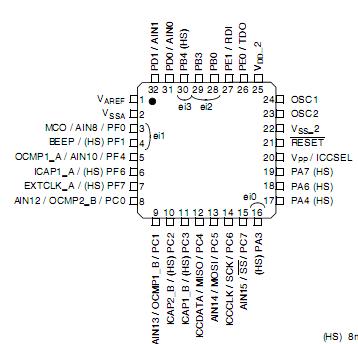
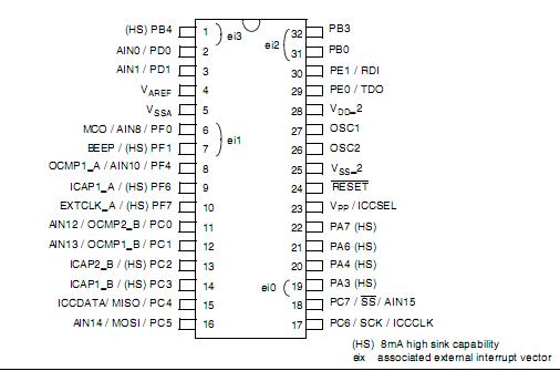
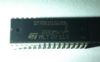
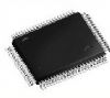
ST72324BL: Features: Memories 8 to 32K dual voltage High Density Flash (HDFlash) or ROM with read-out protection capability. In-Application Programming and In- Circuit Programming for HDFlash devices 384 to 1...

floor Price/Ceiling Price

Part Number:
ST72324BL
Supply Ability:
5000

Price Break

  • Qty
  • 1~5000
  • Unit Price
  • Negotiable
  • Processing time
  • 15 Days
Total Cost: $ 0.00

SeekIC Buyer Protection PLUS - newly updated for 2013!

  • Escrow Protection.
  • Guaranteed refunds.
  • Secure payments.
  • Learn more >>

Month Sales

268 Transactions

Rating

evaluate  (4.8 stars)

Upload time: 2025/12/23

Payment Methods

All payment methods are secure and covered by SeekIC Buyer Protection PLUS.

Notice: When you place an order, your payment is made to SeekIC and not to your seller. SeekIC only pays the seller after confirming you have received your order. We will also never share your payment details with your seller.
Product Details

Description


Features:

Memories
8 to 32K dual voltage High Density Flash (HDFlash) or ROM with read-out protection capability. In-Application Programming and In- Circuit Programming for HDFlash devices
384 to 1K bytes RAM
HDFlash endurance: 100 cycles, data retention:20 years at 55°C
Clock, Reset And Supply Management
Clock sources: crystal/ceramic resonator oscillators,internal RC oscillator, and bypass for external clock
PLL for 2x frequency multiplication
Four Power Saving Modes: Halt, Active-Halt,Wait and Slow
Interrupt Management
Nested interrupt controller
10 interrupt vectors plus TRAP and RESET
9/6 external interrupt lines (on 4 vectors)
Up to 32 I/O Ports
32/24 multifunctional bidirectional I/O lines
22/17 alternate function lines
12/10 high sink outputs
4 Timers
Main Clock Controller with: Real time base,Beep and Clock-out capabilities
Configurable watchdog timer
16-bit Timer A with: 1 input capture, 1 output compare, external clock input, PWM and pulse generator modes
16-bit Timer B with: 2 input captures, 2 output compares, PWM and pulse generator modes
2 Communication Interfaces
SPI synchronous serial interface
SCI asynchronous serial interface
1 Analog Peripheral
10-bit ADC with up to 12 input ports
Instruction Set
8-bit Data Manipulation
63 Basic Instructions
17 main Addressing Modes
8 x 8 Unsigned Multiply Instruction
Development Tools
Full hardware/software development package
In-Circuit Testing capability


Pinout

  Connection Diagram  Connection Diagram  Connection Diagram


Specifications

Voltage Characteristics
Symbol

Ratings Maximum value Unit
VDD - VSS Supply voltage 6.5 V
VPP - VSS Programming Voltage 13
VIN1) & 2) Input Voltage on true open drain pin VSS-0.3 to 5.5
Input voltage on any other pin VSS-0.3 to VDD+0.3
|∆VDDx| and|∆VSSx| Variations between different digital power pins 50 mV
|VSSA - VSSx|
Variations between digital and analog ground pins
50
VESD(HBM) Electro-static discharge voltage (Human Body Model)    
VESD(MM)
Electro-static discharge voltage (Machine Model)
   
Current Characteristics
Symbol

Ratings   Maximum value Unit
IVDD Total current into VDD power lines
(source) 3)
32-pin devices 75 mA
44-pin devices 150
IVSS Total current out of VSS ground lines
(sink) for 3)
32-pin devices 75 mA
44-pin devices 150
IIO Output current sunk by any standard I/O and control pin
25 mA
Output current sunk by any high sink I/O pin 50
Output current source by any I/Os and control pin - 25
IINJ(PIN)2) & 4) Injected current on VPP pin ± 5
Injected current on RESET pin when not driven low internally ± 2
Injected current on flash device pin PB0X ± 2
Injected current on OSC1 and OSC2 pins ± 5
Injected current on any other pin 5) & 6) ± 5
IINJ( 2) Total injected current (sum of all I/O and control pins) 5) ± 25
Thermal Characteristics
Symbol

Ratings Value Unit
TSTG Storage temperature range -65 to +150 °C
TJ Maximum junction temperature


Customers Who Bought This Item Also Bought

Margin,quality,low-cost products with low minimum orders. Secure your online payments with SeekIC Buyer Protection.
Cable Assemblies
Inductors, Coils, Chokes
Motors, Solenoids, Driver Boards/Modules
Sensors, Transducers
Power Supplies - Board Mount
View more