Pinout DescriptionThe ST72P63BK1B1 is designed as one kind of low speed USB 8-bit MCUs with flash/ROM, up to 512 bytes RAM, 8-bit ADC, WDG, timer, SCI & I2c. It is based on an industry-standard 8-bit core and feature an enhanced instruction set.ST72P63BK1B1 has many features. (1)Memories: 4, ...
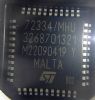
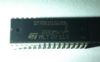
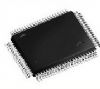
ST72P63BK1B1: Pinout DescriptionThe ST72P63BK1B1 is designed as one kind of low speed USB 8-bit MCUs with flash/ROM, up to 512 bytes RAM, 8-bit ADC, WDG, timer, SCI & I2c. It is based on an industry-standard...
SeekIC Buyer Protection PLUS - newly updated for 2013!
268 Transactions
All payment methods are secure and covered by SeekIC Buyer Protection PLUS.

The ST72P63BK1B1 is designed as one kind of low speed USB 8-bit MCUs with flash/ROM, up to 512 bytes RAM, 8-bit ADC, WDG, timer, SCI & I2c. It is based on an industry-standard 8-bit core and feature an enhanced instruction set.
ST72P63BK1B1 has many features. (1)Memories: 4, 8, or 16Kbytes program memory: high density flash (HDFlash) or ROM with readout and write protection and in-application programming (IAP) and in-circuit programming (ICP) for HDFlash devices and 384 or 512 bytes RAM memory (128-byte stack). (2)Clock, reset and supply management with run, wait, slow and halt CPU modes. (3)USB (universal serial bus) interface: DMA for low speed applications compliant with USB 1.5Mbs (version 1.1) and HID specifications (version 1.0). (4)19 I/O ports. (5)2 timers. (6)2 communication interfaces. (7)1 analog peripheral. (8)Instruction set. (9)Development tools. Those are all the main features.
Some ST72P63BK1B1 absolute maximum ratings have been concluded into several points as follow. (1)Its supply voltage would be 6.0V. (2)Its input voltage on true open drain pins would be from Vss-0.3V to 6.0V. (3)Its input voltage on any other pin would be from Vss-0.3V to Vdd+0.3V. (4)Its total current into Vdd power lines source would be 80mA. (5)Its total current out of Vss ground lines sink would be 80mA. (6)Its output current sunk by any standard I/O and control pin would be 25mA. (7)Its output current sunk by any high sink I/O pin would be 50mA. (8)Its output current source by any I/Os and control pin would be -25mA. (9)Its injected current on Vpp pin would be TBD. (10)Its injected current on /RESET pin would be +/-5mA. (11)Its intected current on OSCIN and OSCOUT pins would be +/-5mA. (12)Its intected current on any other pin would be TBD. (13)Its total intected current (sum of all I/O and control pins) would be +/-20mA. It should be noted that stresses above those listed in absolute maximum ratings may cause permanent damage to device. And so on. If you have any question or suggestion or want to know more ST72P63BK1B1 information please contact us for details. Thank you!