ST7LITE3

Features: · ICP (In-Circuit Programming)· IAP (In-Application Programming)· ICT (In-Circuit Testing) for downloading and executing user application test patterns in RAM· Sector 0 size configurable by option byte· Read-out and write protectionPinoutSpecificationsStresses above those listed as abso...

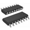
product image

ST7LITE3 Picture
SeekIC No. : 004506845 Detail

ST7LITE3: Features: · ICP (In-Circuit Programming)· IAP (In-Application Programming)· ICT (In-Circuit Testing) for downloading and executing user application test patterns in RAM· Sector 0 size configurable b...

floor Price/Ceiling Price

Part Number:
ST7LITE3
Supply Ability:
5000

Price Break

  • Qty
  • 1~5000
  • Unit Price
  • Negotiable
  • Processing time
  • 15 Days
Total Cost: $ 0.00

SeekIC Buyer Protection PLUS - newly updated for 2013!

  • Escrow Protection.
  • Guaranteed refunds.
  • Secure payments.
  • Learn more >>

Month Sales

268 Transactions

Rating

evaluate  (4.8 stars)

Upload time: 2025/12/23

Payment Methods

All payment methods are secure and covered by SeekIC Buyer Protection PLUS.

Notice: When you place an order, your payment is made to SeekIC and not to your seller. SeekIC only pays the seller after confirming you have received your order. We will also never share your payment details with your seller.
Product Details

Description


Features:

· ICP (In-Circuit Programming)
· IAP (In-Application Programming)
· ICT (In-Circuit Testing) for downloading and executing user application test patterns in RAM
· Sector 0 size configurable by option byte
· Read-out and write protection


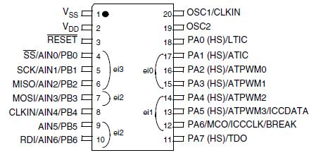
Pinout

  Connection Diagram


Specifications

Stresses above those listed as "absolute maximum ratings" may cause permanent damage to the device. This is a stress rating only and functional operation of the device under these conditions is not implied. Exposure to maximum rating conditions for extended periods may affect device reliability.

Voltage Characteristics

Symbol Ratings Maximum value Unit
VDD - VSS Supply voltage 7.0 V
VIN Input voltage on any pin 1) & 2) VSS-0.3 to VDD+0.3
VESD(HBM) Electrostatic discharge voltage (Human Body Model) see section 13.7.3 on page 143

Current Characteristics
Symbol Ratings
Maximum value
Unit
IVDD Total current into VDD power lines (source) 3)
150
mA
IVSS Total current out of VSS ground lines (sink) 3)
150
IIO Output current sunk by any standard I/O and control pin
25
Output current sunk by any high sink I/O pin
50
Output current source by any I/Os and control pin
-25
IINJ(PIN)2) & 4) Injected current on RESET pin
±5
Injected current on OSC1 and OSC2 pins
±5
Injected current on PB0 and PB1 pins 5)
±5
Injected current on any other pin 6)
±5
IINJ(PIN) 2) Total injected current (sum of all I/O and control pins) 6)
±20

Thermal Characteristics
Symbol Ratings Value Unit
TSTG Storage temperature range -65 to +150
TJ Maximum junction temperature (see section 14.2 on page 156)
Notes:
1. Directly connecting the RESET and I/O pins to VDD or VSS could damage the device if an unintentional internal reset
is generated or an unexpected change of the I/O configuration occurs (for example, due to a corrupted program counter). To guarantee safe operation, this connection has to be done through a pull-up or pull-down resistor (typical: 4.7k for RESET, 10k for I/Os). Unused I/O pins must be tied in the same way to VDD or VSS according to their reset configuration.
2. IINJ(PIN) must never be exceeded. This is implicitly insured if VIN maximum is respected. If VIN maximum cannot be
respected, the injection current must be limited externally to the IINJ(PIN) value. A positive injection is induced by VIN>VDD while a negative injection is induced by VIN<VSS. For true open-drain pads, there is no positive injection current, and the corresponding VIN maximum must always be respected
3. All power (VDD) and ground (VSS) lines must always be connected to the external supply.
4. Negative injection disturbs the analog performance of the device. In particular, it induces leakage currents throughout the device including the analog inputs. To avoid undesirable effects on the analog functions, care must be taken:
   - Analog input pins must have a negative injection less than 0.8 mA (assuming that the impedance of the analog voltage is lower than the specified limits)
  - Pure digital pins must have a negative injection less than 1.6mA. In addition, it is recommended to inject the current as far as possible from the analog input pins.
5. No negative current injection allowed on PB0 and PB1 pins.
6. When several inputs are submitted to a current injection, the maximum IINJ(PIN) is the absolute sum of the positive and negative injected currents (instantaneous values). These results are based on characterisation with IINJ(PIN) maximum current injection on four I/O port pins of the device.


Description

The ST7LITE3 single voltage extended Flash (XFlash) is a non-volatile memory that can be electrically erased and programmed either on a byte-by-byte basis or up to 32 bytes in parallel.

The ST7LITE3 devices can be programmed off-board (plugged in a programming tool) or on-board using In-Circuit Programming or In-Application Programming.

The array matrix organisation of the ST7LITE3 allows each sector to be erased and reprogrammed without affecting other sectors.


Customers Who Bought This Item Also Bought

Margin,quality,low-cost products with low minimum orders. Secure your online payments with SeekIC Buyer Protection.
Crystals and Oscillators
Programmers, Development Systems
Cables, Wires
Connectors, Interconnects
Cables, Wires - Management
View more