Features: ` Memories
2K Bytes single voltage Flash Program memory with read-out protection, In-Circuit and In- Application rogramming (ICP and IAP). 10K write/erase cycles guaranteed, data retention: 20 years at 55°C
128 bytes RAM
128 bytes data EEPROM. 300K write/erase cycles guaranteed, data retention: 20 years at55°C
` Clock, Reset and Supply Management
3-level low voltage supervisor (LVD) and auxiliary voltage detector (AVD) for safe poweron/ off procedures
Clock sources: internal trimmable 8MHz RC oscillator, internal low power, low frequency RC oscillator or external clock
Five Power Saving Modes: Halt, Auto Wake Up from Halt, Active-Halt, Wait and Slow
` Interrupt Management
11 interrupt vectors plus TRAP and RESET
5 external interrupt lines (on 5 vectors)
` I/O Ports
5 multifunctional bidirectional I/O lines
1 additional Output line
6 alternate function lines
5 high sink outputs
` 2 Timers
One 8-bit Lite Timer (LT) with prescaler including: watchdog, 1 realtime base and 1 input capture
One 12-bit Auto-reload Timer (AT) with output compare function and PWM
` A/D Converter
10-bit resolution for 0 to VDD
5 input channels
` Instruction Set
8-bit data manipulation
63 basic instructions with illegal opcode detection
17 main addressing modes
8 x 8 unsigned multiply instruction
` Development Tools
Full hardware/software development package
Debug ModulePinout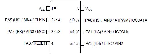 SpecificationsStresses above those listed as "absolute maximum ratings" may cause permanent damage to the device. This is a stress rating only and functional operation of the device under these conditions is not implied. Exposure to maximum rating conditions for extended periods may affect device reliability. 1.Voltage Characteristics
| Symbol |
Symbol |
Symbol |
Unit |
| VDD - VSS |
Supply voltage |
7.0 |
V |
| VIN |
Input voltage on any pin 1) & 2) |
VSS-0.3 to VDD+0.3 |
| VESD(HBM) |
Electrostatic discharge voltage (Human Body Model) |
see section 13.7.2 on page 88 |
| VESD(MM) |
Electrostatic discharge voltage (Machine Model) |
see section 13.7.2 on page 88 |
2. Current Characteristics
| Symbol |
Ratings |
Maximum value |
Unit |
| IVDD |
Total current into VDD power lines (source) 3) |
75 |
mA |
| IVSS |
Total current out of VSS ground lines (sink) 3) |
150 |
| IO |
Output current sunk by any standard I/O and control pin |
20 |
| Output current sunk by any high sink I/O pin |
40 |
| Output current source by any I/Os and control pin |
-25 |
| IINJ(PIN) 2) & 4) |
Injected current on RESET pin |
± 5 |
| Injected current on any other pin 5) |
± 5 |
| IINJ(PIN) 2) |
Total injected current (sum of all I/O and control pins) 5) |
± 20 |
3 .Thermal Characteristics
| Symbol |
Ratings |
Value |
Unit |
| TSTG |
Storage temperature range |
-65 to +150 |
|
| TJ |
Maximum junction temperature (see Section PACKAGE CHARACTERISTICS (Cont'd)) |
Notes:
1. Directly connecting the I/O pins to VDD or VSS could damage the device if an unexpected change of the I/O configuration occurs (for example, due to a corrupted program counter). To guarantee safe operation, this connection has to be done through a pull-up or pull-down resistor (typical: 10k for I/Os). Unused I/O pins must be tied in the same way to VDD or VSS according to their reset configuration.
2. IINJ(PIN) must never be exceeded. This is implicitly insured if VIN maximum is respected. If VIN maximum cannot be
respected, the injection current must be limited externally to the IINJ(PIN) value. A positive injection is induced by VIN>VDD while a negative injection is induced by VIN<VSS.
3. All power (VDD) and ground (VSS) lines must always be connected to the external supply.
4. Negative injection disturbs the analog performance of the device. In particular, it induces leakage currents throughout the device including the analog inputs. To avoid undesirable effects on the analog functions, care must be taken:
- Analog input pins must have a negative injection less than 0.8 mA (assuming that the impedance of the analog voltage is lower than the specified limits)
- Pure digital pins must have a negative injection less than 1.6mA. In addition, it is recommended to inject the current as far as possible from the analog input pins.
5. When several inputs are submitted to a current injection, the maximum IINJ(PIN) is the absolute sum of the positive and negative injected currents (instantaneous values). These results are based on characterisation with IINJ(PIN) maximum current injection on four I/O port pins of the device.
DescriptionThe ST7LITEU09 is a member of the ST7 microcontroller family. All ST7 devices are based on a common industry-standard 8-bit core, featuring an enhanced instruction set.
The ST7LITEU09 features FLASH memory with byte-by-byte In-Circuit Programming (ICP) and In-Application Programming (IAP) capability.
Under software control, the ST7ULTRALITE device can be placed in WAIT, SLOW, or HALT mode, reducing power consumption when the application is in idle or standby state.
The enhanced instruction set and addressing modes of the ST7 offer both power and flexibility to software developers, enabling the design of highly efficient and compact application code. In addition to standard 8-bit data management, all ST7 microcontrollers feature true bit manipulation, 8x8 unsigned multiplication and indirect addressing modes.
For easy reference, all parametric data are located in section 13 on page 74.
The ST7LITEU09 feature an on-chip Debug Module (DM) to support in-circuit debugging (ICD). For a description of the DM registers, refer to the ST7 ICC Protocol Reference Manual.

 ST7LITEU09 Data Sheet