Gate-Source Breakdown Voltage
: +/- 20 V
Configuration
: Single
Maximum Operating Temperature
: + 175 C
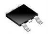
Mounting Style
: SMD/SMT
Transistor Polarity
: P-Channel
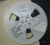
Packaging
: Tube
Continuous Drain Current
: 10 A
Package / Case
: TO-252
Drain-Source Breakdown Voltage
: - 60 V
Resistance Drain-Source RDS (on)
: 0.18 Ohms
Features: ` TYPICAL RDS(on) = 0.18
` EXCEPTIONAL dv/dt CAPABILITY
` 100% AVALANCHE TESTED
` LOW GATE CHARGE
` APPLICATIONORIENTED CHARACTERIZATION
` ADD SUFFIX "T4" FORORDERING IN TAPE & REELApplication· MOTOR CONTROL
· DC-DC & DC-AC CONVERTERSSpecifications
| Symbol |
Parameter |
Value |
Unit |
| VDS |
Collector-Source Voltage (VGS = 0 V) |
60 |
V |
| VDGR |
Drain-gate Voltage (RGS = 20 k) |
60 |
V |
| VGS |
Gate-Source Voltage |
±20 |
V |
| ID |
Drain Current (continuous) at TC = 25 |
10 |
A |
| ID |
Drain Current (continuous) at TC = 100 |
7 |
A |
| IDM(`) |
Drain Current (pulsed) |
40 |
A |
| Ptot |
Total Dissipation at TC = 25 |
40 |
W |
|
Derating Factor |
0.27 |
W/ |
| dv/dt |
Peak Diode Recovery voltage slope |
6 |
V/ns |
| Tstg |
Storage Temperature |
-65 to 175 |
|
| Tj |
Max. Operating Junction Temperature |
175 |
|
(•) Pulse width limited by safe operating area
(1) ISD 10 A, di/dt 300 A/s, VDD V(BR)DSS, Tj TJMAX
Note: For the P-CHANNEL MOSFET actual polarity of voltages and current has to be reversed
DescriptionThe STD10PF06 is a kind of power MOSFET which is the latest development of STMicroelectronics unique single feature size strip-based process. The resulting transistor shows extremely high packing density for low on-resistance, rugged avalanche characteristics and less critical alignment steps therefore a remarkable manufacturing reproducibility.
The features of STD10PF06 can be summarized as (1)typical RDS(on) = 0.18; (2)exceptional dv/dt capability; (3)100% avalanche tested; (4)low gate charge; (5)application oriented characterization; (6)add suffix T4 for ordering in tape & reel.
The absolute maximum ratings of STD10PF06 are (1)VDS drain-source voltage (VGS = 0): 60 V; (2)VDGR drain- gate voltage (RGS = 20 k): 60 V; (3)VGS gate-source voltage: ± 20 V; (4)ID drain current (continuous) at Tc = 25°C: 10 A; (5)ID drain current (continuous) at Tc = 100°C: 7 A; (6)IDM(* Pulse width limited by safe operating area ( 1) I SD 10 A, di/dt 300 A/s, V DD V (BR)DSS , T j T JMAX)/drain current (pulsed): 40 A; (7)Ptot total dissipation at Tc = 25°C: 40 W; (8)derating factor: 0.27 W/°C; (9)dv/dt Peak diode recovery voltage slope: 6 V/ns; (10)Tstg storage temperature: -65 to 175°C; (11)Tj Max. operating junction temperature: 175°C(Note: For the P-CHANNEL MOSFET actual polarity of voltages and current has to be reversed).

 STD10PF06 Data Sheet