STG5682

Features: ` Distortion-free negative signal throughput down to VCC-5.5V` Wide operating voltage range: VCC (Opr) = 1.65V to 4.5V single supply` Ultra low power dissipation: ICC = 0.2A (Max.) at tA = 85°C` Low ON resistance VIN = 0V: RON = 0.5 (max. tA = 25°C) at VCC = 4.3V` 4.3V tolerant and 1.8...

product image

STG5682 Picture
SeekIC No. : 004507620 Detail

STG5682: Features: ` Distortion-free negative signal throughput down to VCC-5.5V` Wide operating voltage range: VCC (Opr) = 1.65V to 4.5V single supply` Ultra low power dissipation: ICC = 0.2A (Max.) at tA =...

floor Price/Ceiling Price

Part Number:
STG5682
Supply Ability:
5000

Price Break

  • Qty
  • 1~5000
  • Unit Price
  • Negotiable
  • Processing time
  • 15 Days
Total Cost: $ 0.00

SeekIC Buyer Protection PLUS - newly updated for 2013!

  • Escrow Protection.
  • Guaranteed refunds.
  • Secure payments.
  • Learn more >>

Month Sales

268 Transactions

Rating

evaluate  (4.8 stars)

Upload time: 2024/4/28

Payment Methods

All payment methods are secure and covered by SeekIC Buyer Protection PLUS.

Notice: When you place an order, your payment is made to SeekIC and not to your seller. SeekIC only pays the seller after confirming you have received your order. We will also never share your payment details with your seller.
Product Details

Description


Features:

` Distortion-free negative signal throughput down to VCC-5.5V
` Wide operating voltage range: VCC (Opr) = 1.65V to 4.5V single supply
` Ultra low power dissipation: ICC = 0.2A (Max.) at tA = 85°C
` Low "ON" resistance VIN = 0V: RON = 0.5 (max. tA = 25°C) at VCC = 4.3V
` 4.3V tolerant and 1.8V compatible threshold on digital control input at VCC = 1.65 to 3.0V
` Latch-up performance exceeds 300mA (JESD 17)
` ESD performance exceeds JESD22
` 2000-V human-body model (A114-A)


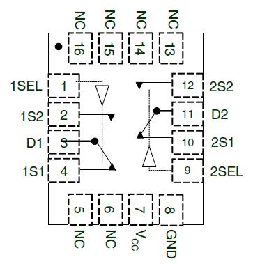
Pinout

  Connection Diagram


Specifications

Symbol
Conditions
Value
Unit
VCC
Supply voltage
-0.5 to 5.5
V
VI
DC input voltage
-(VCC - 6.0V) to
VCC + 0.5
V
VIC
DC control input voltage
-0.5 to 5.5
V
VO
DC output voltage
-(VCC - 6.0V) to
VCC + 0.5
V
IIKC
DC input diode current on control pin (VSEL<0V)
-50
mA
IIK
DC input diode current (VSE<0V)
±50
mA
IOK
DC output diode current
±20
mA
IO
DC output current
±150
mA
IOP
DC output current peak (pulse at 1ms, 10% duty cycle)
±400
mA
ICCOR
IGND
DC VCC or ground current
±100
mA
PD
Power dissipation at TA = 70 (1)
1120
mW
TSTG
Storage temperature
-65 to +150
TJ
Lead temperature (10 sec)
300


Description

The STG5682 is a high-speed CMOS low voltage dual analog S.P.D.T. (Single Pole Dual Throw) SWITCH or 2:1 Multiplexer /Demultiplexer Switch fabricated in silicon gate C2MOS technology. It is designed to operate from 1.65V to 4.5V, making this device ideal for portable applications.

Additional key features of STG5682 are fast switching speed, Break Before Make Delay Time and Ultra Low Power Consumption. All inputs and outputs are equipped with protection circuits against static discharge, giving them ESD immunity and transient excess voltage.


Customers Who Bought This Item Also Bought

Margin,quality,low-cost products with low minimum orders. Secure your online payments with SeekIC Buyer Protection.
Computers, Office - Components, Accessories
Transformers
Connectors, Interconnects
Semiconductor Modules
Soldering, Desoldering, Rework Products
View more