STLVD112

ApplicationThe STLVD112 is a low voltage differential to LVTTL signal converter with enhanced loop-back and crosspoint features. The synchronous design allows a phase alignment between a clock and its data; this means a better BER (Bit Error Rate) performance.The advanced 0.35m technology makes th...

product image

STLVD112 Picture
SeekIC No. : 004508112 Detail

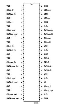
STLVD112: ApplicationThe STLVD112 is a low voltage differential to LVTTL signal converter with enhanced loop-back and crosspoint features. The synchronous design allows a phase alignment between a clock and i...

floor Price/Ceiling Price

Part Number:
STLVD112
Supply Ability:
5000

Price Break

  • Qty
  • 1~5000
  • Unit Price
  • Negotiable
  • Processing time
  • 15 Days
Total Cost: $ 0.00

SeekIC Buyer Protection PLUS - newly updated for 2013!

  • Escrow Protection.
  • Guaranteed refunds.
  • Secure payments.
  • Learn more >>

Month Sales

268 Transactions

Rating

evaluate  (4.8 stars)

Upload time: 2025/12/24

Payment Methods

All payment methods are secure and covered by SeekIC Buyer Protection PLUS.

Notice: When you place an order, your payment is made to SeekIC and not to your seller. SeekIC only pays the seller after confirming you have received your order. We will also never share your payment details with your seller.
Product Details

Description


Application

The STLVD112 is a low voltage differential to LVTTL signal converter with enhanced loop-back and crosspoint features. The synchronous design allows a phase alignment between a clock and its data; this means a better BER (Bit Error Rate) performance.

The advanced 0.35m technology makes the STLVD112 suitable for data rates up to 200Mbit.The main application field is SDH/SONET telecom infrastructure. The STLVD112 flexible switch architecture makes it easy to implement multiple protection schemes in STM1 access systems.Thanks to the flexible multiplexing allowed, it becomes simple to redirect the data/clock signal coming from the faulty access card to the spare card. In normal mode the STLVD112 converts the differential data levels of the LVDS and relatedclock signal from (to) the line interface in LVTTL level signals to (from) the backpanel. In addition the switch functions prevent the equipment from line interface faults. In fact, it is possible to switch the signals coming from a different line interface to the local line interface or the signals from the local line interface to a different line interface.


Pinout

  Connection Diagram


Specifications

Symbol Parameter Value Unit
VS1, VS2 Supply Voltage -0.3 to 4.6 V
VS2 Supply Voltage -0.3 to (VS1 + 0.3) V
VI DC Input Voltage -0.3 to (VS1 + 0.3) V
VO DC Output Voltage -0.3 to (VS1 + 0.3) V
Iik DC Input Diode Clamp Current ±20 mA
Iok DC Output Diode Clamp Current ±20 mA
IO DC Output Current ±50 mA
TL Lead  Temperature (10sec) 300
Tstg Storage Temperature Range -65 to 150


Description

The features of STLVD112:

 24mA CMOS OUTPUT DRIVE CURRENT
LVTTL INPUT THRESHOLDS
CONTROLLED SKEW BETWEEN DATA AND CLOCK SIGNALS
LVDS INPUT-OUTPUT UP TO 155 MHZ
IMPROVED LATCH-UP IMMUNITY UP TO 300mA


Customers Who Bought This Item Also Bought

Margin,quality,low-cost products with low minimum orders. Secure your online payments with SeekIC Buyer Protection.
Connectors, Interconnects
Cable Assemblies
Inductors, Coils, Chokes
Optical Inspection Equipment
Undefined Category
View more