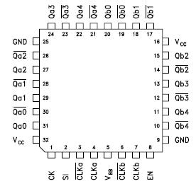
Features: 100ps PART-TO-PART SKEW50ps BANK SKEWDIFFERENTIAL DESIGNMEETS LVDS SPEC. FOR DRIVER OUTPUTS AND RECEIVER INPUTSREFERENCE VOLTAGE AVAILABLE OUTPUT VBBLOW VOLTAGE VCC RANGE OF 2.375V TO 2.625VHIGH SIGNALLING RATE CAPABILITY (EXCEEDS 700MHz)SUPPORT OPEN, SHORT, ANDTERMINATED INPUT FAIL-SAFE...
STLVD210: Features: 100ps PART-TO-PART SKEW50ps BANK SKEWDIFFERENTIAL DESIGNMEETS LVDS SPEC. FOR DRIVER OUTPUTS AND RECEIVER INPUTSREFERENCE VOLTAGE AVAILABLE OUTPUT VBBLOW VOLTAGE VCC RANGE OF 2.375V TO 2.62...
SeekIC Buyer Protection PLUS - newly updated for 2013!
268 Transactions
All payment methods are secure and covered by SeekIC Buyer Protection PLUS.

| Symbol | Parameter | Value | Unit |
| VCC | Supply Voltage | -0.3 to 2.8 | V |
| VI | Input Voltage | -0.2 to (VCC+0.2) | V |
| VO | Output Voltage | -0.2 to (VCC+0.2) | V |
| IOSD | Driver Short Circuit Current | Continuous | |
| ESD | Electrostatic Discharge (HBM 1.5K, 100pF) | >2 | KV |
The STLVD210 is a low skew programmable 1-to-5 dual differential LVDS driver, designed with clock distribution in mind. The LVDS input signals can be either differential or single-ended if the VBB output is used.
The STLVD210 is provided with a 11 bit shift register with a serial in and a Control Register.The purpose is to enable or power off each output clock channel and to select the clock input. The STLVD210 is specifically designed, modelled and produced with low skew as the key goal. Optimal design and layout serve to minimize gate to gate skew within a device. The net result is a dependable guaranteed low skew device.
The STLVD210 can be used for high performance clock distribution in 2.5V systems with LVDS levels. Designers can be take advantage of the device's performance to distribute low skew clocks across the backplane or the board.