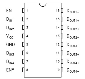
Features: >400 MBPS (200MHZ) SWITCHING RATESFLOW-THROUGH PINOUT SIMPLIFIES PCB LAYOUT300ps (MAX.) DIFFERENTIAL SKEW1.8 ns (TYP.) PROPAGATION DELAY3.3V POWER SUPPLY DESIGN±350 mV DIFFERENTIAL SIGNALINGLOW POWER DISSIPATION (3.5mW AT 3.3V STATIC IN TRISTATE)INTEROPERABLE WITH EXISTING 5V LVDS REC...
STLVDS47: Features: >400 MBPS (200MHZ) SWITCHING RATESFLOW-THROUGH PINOUT SIMPLIFIES PCB LAYOUT300ps (MAX.) DIFFERENTIAL SKEW1.8 ns (TYP.) PROPAGATION DELAY3.3V POWER SUPPLY DESIGN±350 mV DIFFERENTIAL SIGN...
SeekIC Buyer Protection PLUS - newly updated for 2013!
268 Transactions
All payment methods are secure and covered by SeekIC Buyer Protection PLUS.
>400 MBPS (200MHZ) SWITCHING RATES
FLOW-THROUGH PINOUT SIMPLIFIES PCB LAYOUT
300ps (MAX.) DIFFERENTIAL SKEW
1.8 ns (TYP.) PROPAGATION DELAY
3.3V POWER SUPPLY DESIGN
±350 mV DIFFERENTIAL SIGNALING
LOW POWER DISSIPATION (3.5mW AT 3.3V STATIC IN TRISTATE)
INTEROPERABLE WITH EXISTING 5V LVDS RECEIVERS
HIGH IMPEDANCE ON LVDS OUTPUT ON POWER DOWN
CONFORMS TO TIA/EIA-644 LVDS STANDARD
INDUSTRIAL OPERATING TEMPERATURE RANGE (-40 °C TO +85 °C)
AVAILABLE IN SURFACE MOUNT (SOIC) AND LOW PROFILE TSSOP PACKAGE

| Symbol | Parameter | Value | Unit |
| VCC | Supply Voltage | -0.3 to 4 | V |
| DIN | Input Voltage | -0.3 to 6 | V |
| EN, EN* | Enable Input Voltage | -0.3 to 6 | V |
| DOUT+,DOUT- | Output Voltage | -0.3 to 3.9 | V |
| ISCTOUT | Short Circuit Duration | Continuous | |
| Tstg | Storage Temperature Range | -65 to +150 | °C |
The STLVDS47 is a quad CMOS flow-through differential line driver designed for applications requiring ultra low power dissipation and high data rate. The device is designed to support data rates in excess of 400Mbps (200 MHz) utilizing Low Voltage Differential Signaling (LVDS) techology.The STLVDS47 accepts low voltage TTL/CMOS input levels and translates them to low voltage (350 mV) differential output signals. In addition,the driver support a TRI-STATE function that may be used to disable the output stage, disabling the load current, and thus dropping the device to an
ultra low idle power state of 1.3mW typical. The STLVDS47 has a flow-through pinout for easy PCB layout.
The EN and EN* inputs are ANDed together and control the TRI-STATE output.The STLVDS47 and companion line receiver (STLVDS48) provide a new alternative to high power pseudo-ECL devices for high-speed point-to-point interface applications.