Features: ` Core: ARM 32-bit Cortex™-M3 CPU
36 MHz, 45 DMIPS with 1.25 DMIPS/MHz
Single-cycle multiplication and hardware division
Nested interrupt controller with 43 maskable interrupt channels
Interrupt processing (down to 6 CPU cycles) with tail chaining
` Memories
32-to-128 Kbytes of Flash memory
6-to-16 Kbytes of SRAM
` Clock, reset and supply management
2.0 to 3.6 V application supply and I/Os
POR, PDR and programmable voltage detector (PVD)
4-to-16 MHz high-speed quartz oscillator
Internal 8 MHz factory-trimmed RC
Internal 32 kHz RC
PLL for CPU clock
Dedicated 32 kHz oscillator for RTC with calibration
` Low power
Sleep, Stop and Standby modes
VBAT supply for RTC and backup registers
` Debug mode
Serial wire debug (SWD) and JTAG interfaces
` DMA
7-channel DMA controller
Peripherals supported: timers, ADC, SPIs, I2Cs and USARTs
` 12-bit, 1 µs A/D converter (16-channel)
Conversion range: 0 to 3.6 V
Temperature sensor
` Up to 80 fast I/O ports
32/49/80 5 V-tolerant I/Os
All mappable on 16 external interrupt vectors
Atomic read/modify/write operations
` Up to 6 timers
Up to three 16-bit timers, each with up to 4 IC/OC/PWM or pulse counter
2 x 16-bit watchdog timers (Independent and Window)
SysTick timer: 24-bit downcounter
` Up to 7 communication interfaces
Up to 2 x I2C interfaces (SMBus/PMBus)
Up to 3 USARTs (ISO 7816 interface, LIN, IrDA capability, modem control)
Up to 2 SPIs (18 Mbit/s)Pinout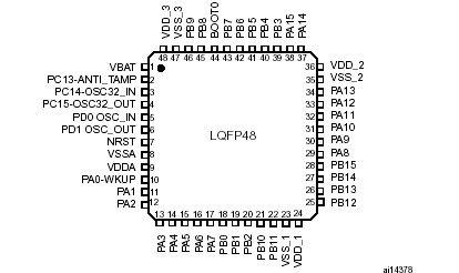
Specifications
|
Symbol |
Ratings |
Min |
Max |
Unit |
|
VDD−VSS |
External 3.3 V supply voltage (including
VDDA and VDD)(1) |
0.3 |
4.0 |
V |
|
VIN |
Input voltage on five volt tolerant pin(2) |
VSS − 0.3 |
+5.5 |
| Input voltage on any other pin(2) |
VSS − 0.3 |
VDD+0.3 |
|
|∆VDDx| |
Variations between different power pins |
50 |
50 |
mV |
|
|VSSX − VSS| |
Variations between all the different ground pins |
50 |
50 |
|
VESD(HBM) |
Electrostatic discharge voltage (human
body model) |
see Section 5.3.11: Absolute
maximum ratings (electrical
sensitivity) |
|
1. All 3.3 V power (V
DD, V
DDA) and ground (V
SS, V
SSA) pins must always be connected to the external 3.3 V supply.
2. IINJ(PIN) must never be exceeded (see Table 5: Current characteristics). This is implicitly insured if V
IN maximum
is respected. If V
IN maximum cannot be respected, the injection current must be limited externally to the I
IN
J(PIN) value. A positive injection is induced by V
IN>V
DD while a negative injection is induced by V
IN<V
SS.
DescriptionThe STM32F101x8 access line family incorporates the high-performance ARM Cortex™-M3 32-bit RISC core operating at a 36 MHz frequency, high-speed embedded memories (Flash memory up to 128Kbytes and SRAM up to 16 Kbytes), and an extensive range of enhanced peripherals and I/Os connected to two APB buses. All STM32F101x8 offer standard communication interfaces (two I2Cs, two SPIs, and up to three USARTs), one 12-bit ADC and three general
purpose 16-bit timers.
The STM32F101x8 family operates in the −40 to +85°C temperature range, from a 2.0 to 3.6 V power supply. A comprehensive set of power-saving mode allows to design low-power applications.
The complete STM32F101x8 access line family includes devices in 3 different package types: from 48 pins to 100 pins. Depending on the device chosen, different sets of peripherals are included, the description below gives an overview of the complete range of peripherals proposed in this family.
These features make the STM32F101x8 access line microcontroller family suitable for a wide range of applications:
· Application control and user interface
· Medical and handheld equipment
· PC peripherals, gaming and GPS platforms
· Industrial applications: PLC, inverters, printers, and scanners
· Alarm systems, Video intercom, and HVAC

 STM32F101x8 Data Sheet