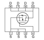
Features: Super high dense cell design for low RDS (ON).Rugged and reliable.Surface Mount Package.PinoutSpecifications Parameter Symbol Limit Unit Drain-S ource Voltage VDS 30 V Gate-S ource Voltage VGS 20 V Drain Current-Continuousa @ TJ=25 -Pulsedb ID 12 A IDM 4...
STM4884A: Features: Super high dense cell design for low RDS (ON).Rugged and reliable.Surface Mount Package.PinoutSpecifications Parameter Symbol Limit Unit Drain-S ource Voltage VDS 30 V ...
SeekIC Buyer Protection PLUS - newly updated for 2013!
268 Transactions
All payment methods are secure and covered by SeekIC Buyer Protection PLUS.

| Parameter | Symbol | Limit | Unit |
| Drain-S ource Voltage | VDS | 30 | V |
| Gate-S ource Voltage | VGS | 20 | V |
| Drain Current-Continuousa @ TJ=25 -Pulsedb | ID | 12 | A |
| IDM | 44 | A | |
| Drain-S ource Diode Forward Currenta | IS | 1.7 | A |
| Maximum Power Dissipationa | PD | 2.5 | W |
| Operating Junction and S torage Temperature R ange |
TJ , TSTG | -55 to 150 | G |
The features of STM4884A: (1)super high dense cell design for low RDS(on); (2)rugged and reliable; (3)suface mount package.
The absolute maximum ratings of the STM4884A are: (1)drain-source voltage: 30V; (2)gate-source voltage: ±20V; (3)drain current-continuous: 12A; (4)drain-source diode forward current: 1.7A; (5)maximum power dissipation: 2.5W; (6)operating junction and storage: -55 to 150; (7)temperature range: -55 to 150.
The following is about the maximum ratings of STM4884A: (1)Drain-Source Breakdown Voltage: 30V at VGS = 0V, ID = 250uA; (2)Zero Gate Voltage Drain Current: 1 uA at VDS = 24V, VGS = 0V; (3)Gate-Body Leakage: ±100 nA at VGS = ±20V, VDS = 0V; (4)Gate Threshold Voltage: 1V min, 1.6V typical and 3V max at VDS = VGS , ID = 250uA; (5)Drain-Source On-State Resistance: 6mobm at VGS 10V, ID 12A; (6)On-State Drain Current: 20A min at VDS = 10V, VGS = 10V; (7)Forward Transconductance: 22S at VDS 15V, ID=12A.