Features: MAIN SWITCHES MAX. RON LESS THAN 2 PROVIDES 7 AUXILIARY SWITCHES WITH RON < 75 6VPP AMPLITUDE OF ANALOG INPUT SIGNAL DIGITAL INPUTS ARE TTL LEVELS COMPATIBLE PinoutSpecifications Symbol Description Min Max Unit VPOS Positive Power Supply Voltage VNEG - 0.3 VNEG + 7...
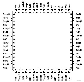
STM7E1A: Features: MAIN SWITCHES MAX. RON LESS THAN 2 PROVIDES 7 AUXILIARY SWITCHES WITH RON < 75 6VPP AMPLITUDE OF ANALOG INPUT SIGNAL DIGITAL INPUTS ARE TTL LEVELS COMPATIBLE PinoutSpecifications S...
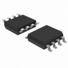
SeekIC Buyer Protection PLUS - newly updated for 2013!
268 Transactions
All payment methods are secure and covered by SeekIC Buyer Protection PLUS.

| Symbol | Description | Min | Max | Unit |
| VPOS | Positive Power Supply Voltage | VNEG - 0.3 | VNEG + 7 | V |
| GND | Reference Ground | VNEG - 0.3 | VNEG + 7 | V |
| VIN | Input Voltage for Digital Inputs and Analog Input/Output Pins |
VNEG - 0.3 | VNEG + 7 | V |
The STM7E1A consists in 7 identical ISDN E1 channels, each channel corresponding to 4 main low-resistant switches (a and b) and 2 auxiliary switches (c and d). The switches positions in all the channels are identical and controlled by a unique control resource driven by the digital inputs Lm, Ls and Sc.
In each STM7E1A channel, the TX and RX lines can be switched between a Main port or a Spare-port by the main switches: if both "a" switches are closed and both "b" switches are open, the Main port is connected to the line, while if both "a" switches are open and both "b' switches are closed, the spare port is connected to the line.
The 2 auxiliary switches enable to close a local loop between the TX and RX access of a port: if "c" is closed, the Spare port RX and TX access is connected between each other to form a local loop, while if "d" is closed, the Main port RX and TX access is connected between each other to form a local loop.
The STM7E1A Spare port is only used for test purpose on the system board while the Main port is the communication channel. Consequently, a switching from the Main port to the Spare port occurs very rarely (<10 times a day).The power supplies of the chip need to be de coupled properly. This means that at least one external capacitor C1 must be connected in between GND and VPOS, one external capacitor C2 between GND and VNEG, and one external capacitor C3 between each pair of VNEG and VPOS.