DescriptionThe STR-S5141G is designed as sanken switching regulator hybrid IC which is base on the silicon 3-layer planar transistor. drive circuit and reference voltage circuit are built in. Typical applications is switching regulator for RCC type TV.Some absolute maximum ratings of STR-S5141Ghav...
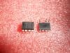
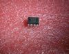
STR-S5141G: DescriptionThe STR-S5141G is designed as sanken switching regulator hybrid IC which is base on the silicon 3-layer planar transistor. drive circuit and reference voltage circuit are built in. Typica...
SeekIC Buyer Protection PLUS - newly updated for 2013!
268 Transactions
All payment methods are secure and covered by SeekIC Buyer Protection PLUS.
The STR-S5141G is designed as sanken switching regulator hybrid IC which is base on the silicon 3-layer planar transistor. drive circuit and reference voltage circuit are built in. Typical applications is switching regulator for RCC type TV.
Some absolute maximum ratings of STR-S5141G have been concluded into several points as follow. (1)Its collector to emitter voltage would be 500V. (2)Its applied voltage of pin #2-#4 would be 12V. (3)IIts applied voltage of pin #2-#5 would be 12V. (4)Its applied voltage of pin #7-#6 would be 5V. (5)Its Tr1 collector current would be 10A for continuous and would be 20A for pulse. (6)Its Tr4 collector current would be 500mA. (7)Its D2 forward current would be 500mA. (8)Its maximum power dissipation would be 3.2W without heatsink and would be 2.7W at Tc1=100°C. (9)Its junction temperature would be 150°C. (10)Its operating frame temperature range would be from -20°C to 125°C. (11)Its storage temperature range would be from -30°C to 125°C. (12)Its maximum output current would be 1.7A at Vo=115V. It should be noted that stresses above those listed in absolute maximum ratings may cause permanent damage to device.
Also some electrical characteristics of STR-S5141G are concluded as follow. (1)Its reference voltage would be 41.8+/-0.3V with test conditions of Iin=7mA, circuit 1. (2)Its temperature coefficient of reference voltage would be typ +/-2mV/°C with test conditions of Tc=-20°C to 100°C and Iin=7mA and circuit 1. (3)Its collector saturation voltage would be max 0.5V with test conditions of Ic=6A and Ib=1.2A. (4)Its collector cutoff voltage would be max 1mA with test conditions of Vce=500V and Vbe=-1.5V. (5)Its base to emitter saturation voltage would be max 1.5V. (6)Its DC current gain would be min 15 and max 40. (7)Its thermal resistance would be 0.7°C/W. (8)Its switching time would be max 10us for ts and would be max 0.6us for tr. And so on. If you have any question or suggestion or want to know more information please contact us for details. Thank you!