Features: ` Core
ARM7TDMI-S 32-bit RISC CPU
54 DMIPS @ 60 MHz
` Memories
Up to 256 KB Flash program memory (10k erase/write cycles, retention 20 yrs at 85°C)
16KB Read-While-Write Flash for data (100k erase/write cycles, retention 20 yrs@ 85°C)
Flash Data Readout and Write Protection
16KBytes embedded high speed SRAM
Memory mapped interface (SMI) to ext.
Serial Flash (64 MB) w. boot capability
` Clock, Reset and Supply Management
Single supply 3.3V ±10% or 5V ±10%
Embedded 1.8V Voltage Regulators with Low Power features
Smart Clock Controller with flexible clock generation capability:
Internal RC for fast start-up and backup clock mechanism
Up to 60 MHz operation using internal PLL with 4 or 8 MHz crystal/ceramic osc.
Smart Low Power Modes: SLOW, WFI, STOP and STANDBY with backup registers
Real Time Clock, driven by low power internal RC or 32.768 kHz dedicated osc, for clock-calendar and Auto Wake-up
` Nested interrupt controller
Fast interrupt handling with 32 vectors
16 IRQ priorities, 2 maskable FIQ sources
16 external interrupt / wake-up Lines
` DMA
4-channel DMA controller
Circular buffer management
Support for UART, SSP, Timers, ADC
` 6 Timers
16-bit watchdog timer (WDG)
16-bit timer for system timebase functions
3 synchronizable timers each with up to 2 input captures and 2 output compare/PWMs.
16-bit 6-channel synchronizable PWM timer
Dead time generation, edge/center-aligned waveforms and emergency stop
Ideal for induction/brushless DC motors
` 8 Communications Interfaces
1 I2C interface
3 HiSpeed UARTs w. Modem/LIN capability
2 SSP interfaces (SPI or SSI) up to 16 Mb/s
1 CAN interface (2.0B Active)
1 USB full-speed 12 Mb/s interface with 8 configurable endpoint sizes
` 10-bit A/D Converter
16/11 chan. with prog. Scan Mode & FIFO
Programmable Analog Watchdog feature
Conversion: min. 3.75 s, range: 0 to VDD_IO
Start conversion can be triggered by timers
` Up to 72/38 I/O ports
72/38 GPIO lines with High Sink capabilities
Atomic bit SET and RES operationsPinout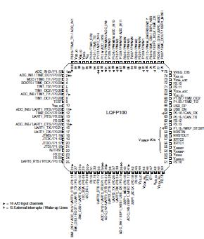 Specifications
Stresses above those listed as "absolute maximum ratings" may cause permanent damage to the device. This is a stress rating only and functional operation of the device under these conditions is not implied. Exposure to maximum rating conditions for extended periods may affect device reliability.
Voltage characteristics
| Symbol |
Ratings |
Min |
Max |
Unit |
| VDD_x - VSS_X (1) |
Including VDDA_ADC and VDDA_PLL |
-0.3 |
6.5 |
V |
| V18 - VSS18 |
Digital 1.8 V Supply voltage on all V18
power pins (when 1.8 V is provided
externally) |
-0.3 |
2.0 |
|
| VIN |
Input voltage on any pin (2) |
VSS-0.3 to
VDD_IO+0.3 |
VSS-0.3 to
VDD_IO+0.3 |
|
| |VDDx| |
Variations between different 3.3 V or
5.0 V power pins |
|
50 |
mV |
| |V18x| |
Variations between different 1.8 V power
pins(3) |
|
25 |
| |VSSX - VSS| |
Variations between all the different
ground pins |
|
50 |
| VESD(HBM) |
Electro-static discharge voltage (Human
Body Model) |
see : Absolute
Maximum
Ratings
(Electrical
Sensitivity) on
page 52 |
see : Absolute
Maximum
Ratings
(Electrical
Sensitivity) on
page 52 |
|
| VESD(MM) |
Electro-static discharge voltage (Machine Model) |
|
1. All 3.3 V or 5.0 V power (VDD_IO, VDDA_ADC, VDDA_PLL) and ground (VSS_IO, VSSA_ADC, VDDA_ADC) pins must always be connected to the external 3.3V or 5.0V supply. When powered by 3.3V, I/Os are not 5V tolerant.
2. IINJ(PIN) must never be exceeded. This is implicitly insured if VIN maximum is respected. If VIN maximum cannot be respected, the injection current must be limited externally to the IINJ(PIN) value. A positive injection is induced by VIN>VDD while a negative injection is induced by VIN<VSS. For true open-drain pads,there is no positive injection current, and the corresponding VIN maximum must always be respected 3. Only when using external 1.8 V power supply. All the power (V18, V18REG, V18BKP) and ground (VSS18,VSSBKP) pins must always be connected to the external 1.8 V supply.
3. Only when using external 1.8 V power supply. All the power (V18, V18REG, V18BKP) and ground (VSS18,VSSBKP) pins must always be connected to the external 1.8 V supply.
Current characteristics
| Symbol |
Ratings |
Maximum value |
Unit |
| IVDD_IO (1) |
Total current into VDD_IO power lines (source) (2) |
150 |
mA |
| IVSS_IO (1) |
Total current out of VSS ground lines (sink)(2) |
150 |
| IIO |
Output current sunk by any I/O and control pin |
25 |
| Output current source by any I/Os and control pin |
-25 |
| IINJ(PIN)3) & 4) |
Injected current on NRSTIN pin |
± 5 |
| Injected current on XT1 and XT2 pins |
± 5 |
| Injected current on any other pin (5) |
± 5 |
| IINJ(PIN) 2) |
Total injected current (sum of all I/O and control pins) 5) |
± 25 |
1. The user can use GPIOs to source or sink high current (up to 20 mA for O8 type High Sink I/Os). In this case, the user must ensure that these absolute max. values are not exceeded (taking into account the RUN power consumption) and must follow the rules described in Section 3.3.8: I/O port pin characteristics on page 53.
2. All 3.3 V or 5.0 V power (VDD_IO, VDDA_ADC, VDDA_PLL) and ground (VSS_IO, VSSA_ADC, VDDA_ADC) pins must always be connected to the external 3.3V or 5.0V supply.
3. IINJ(PIN) must never be exceeded. This is implicitly insured if VIN maximum is respected. If VIN maximum cannot be respected, the injection current must be limited externally to the IINJ(PIN) value. A positive injection is induced by VIN>VDD while a negative injection is induced by VIN<VSS.
4. Negative injection disturbs the analog performance of the device. See note in Section 3.3.12: 10-bit ADC
characteristics on page 64.
5. When several inputs are submitted to a current injection, the maximum IINJ(PIN) is the absolute sum of the
positive and negative injected currents (instantaneous values). These results are based on characterization with IINJ(PIN) maximum current injection on four I/O port pins of the device.
Thermal characteristics
| Symbol |
Ratings |
Value |
Unit |
| TSTG |
Storage temperature range |
-65 to +150 |
|
| TJ |
Maximum junction temperature (see Section 42: Thermal characteristics on page 70) |
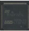
DescriptionThis Datasheet contains the description of the STR750 family STR750F features, pinout, Electrical Characteristics, Mechanical Data and Ordering information.
For complete information on the Microcontroller memory STR750F, registers and peripherals. Please refer to the STR750 Reference Manual.
For information on the ARM7TDMI-S STR750F core please refer to the ARM7TDMI-S Technical Reference Manual available from Arm Ltd.
For information on programming, erasing and protection of the internal Flash memory please refer to the STR7 Flash Programming Reference Manual For information on third-party development tools, please refer to the http://www.st.com/mcu website.

 STR750F Data Sheet