Features: 3.3V and 5V power supply options500ps propagation delayFully differential designSupports both standard and low voltage operationAvailable in 20-pin SOIC packagePinoutDescriptionThe SY100EL90V is a triple ECL/LVECL-to-PECL/ LVPECL translator. The device can translate over all combinations...
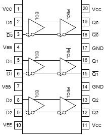
SY100EL90V: Features: 3.3V and 5V power supply options500ps propagation delayFully differential designSupports both standard and low voltage operationAvailable in 20-pin SOIC packagePinoutDescriptionThe SY100EL...
SeekIC Buyer Protection PLUS - newly updated for 2013!
268 Transactions
All payment methods are secure and covered by SeekIC Buyer Protection PLUS.
DescriptionThe SY10/100E111 are low skew 1-to-9 differential drivers designed for clock distributi...
3.3V and 5V power supply options
500ps propagation delay
Fully differential design
Supports both standard and low voltage operation
Available in 20-pin SOIC package

The SY100EL90V is a triple ECL/LVECL-to-PECL/ LVPECL translator. The device can translate over all combinations of supply voltages: -5V ECL to 5V PECL, -5V ECL to 3.3V LVPECL, -3.3V LVECL to 5V PECL or -3.3V LVECL to 3.3V LVPECL.
A VBB output of SY100EL90V is provided for interfacing with single ended ECL signals at the input. If a single ended input is to be used, the VBB output should be connected to the D input. The active signal would then drive the D input. When used, the VBB output should be bypassed to via a 0.01F capacitor. The VBB output is designed to act as the switching reference for the EL90V under single ended input switching conditions. As a result this pin can only source/sink up to 0.5mA of current.
To accomplish the level translation the SY100EL90V requires three power rails. The VCC supply should be connected to the positive supply, and the VEE pin should be connected to the negative power supply. The GND pins as expected are connected to the system ground plane. Both VEE and VCC should be bypassed to ground via 0.01F capacitors.
Under open input conditions, SY100EL90V, the D input will be biased at VCC/2 and the D input will be pulled to VEE. This condition will force the Q output to a LOW, ensuring stability.