Features: 2.5V and 3.3V power supply options Guaranteed AC parameters over temperature: fMAX = 3GHz,< 25ps output-to-output skew,< 250ps tr / tf,< 400ps propagation delay Wide temperature range: 40°C to +85°C Differential design VBB output for single-ended input applications Fully compat...
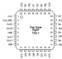
SY100EP111U: Features: 2.5V and 3.3V power supply options Guaranteed AC parameters over temperature: fMAX = 3GHz,< 25ps output-to-output skew,< 250ps tr / tf,< 400ps propagation delay Wide temperature ...
SeekIC Buyer Protection PLUS - newly updated for 2013!
268 Transactions
All payment methods are secure and covered by SeekIC Buyer Protection PLUS.
DescriptionThe SY10/100E111 are low skew 1-to-9 differential drivers designed for clock distributi...
2.5V and 3.3V power supply options
Guaranteed AC parameters over temperature: fMAX = 3GHz, < 25ps output-to-output skew,< 250ps tr / tf,< 400ps propagation delay
Wide temperature range: 40°C to +85°C
Differential design
VBB output for single-ended input applications
Fully compatible with industry standard 100K I/O levels
Available in 32-pin TQFP package

| Symbol | Rating | Value | Unit |
| VCC VEE | Power Supply Voltage (VEE = 0) | +6.0 to 0 | V |
| VIN | Input Voltage (VCC = 0V, VIN not more negative than VEE) Input Voltage (VEE = 0V, VIN not more positive than VCC) |
-6.0 to 0 +6.0 to 0 |
V |
| IOUT | Output Current Continuous Surge |
50 100 |
mA |
| IBB | VBB Sink/Source Current(2) | ±0.5 | mA |
| TA | Operating Temperature Range | -40 to +85 | °C |
| TSTORE | Storage Temperature Range | -65 to +150 | °C |
| JA | Thermal Resistance (Junction-to-Ambient) Still Air 500lfp |
160 109 |
°C/W |
| JC | Thermal Resistance (Junction-to-Case) | 39 | °C/W |
The SY100EP111U is a high-speed, low skew 1-to-10 differential fanout buffer designed for clock distribution in new, high-performance systems. The internal 2:1 mux allows the input to select between two differential clock sources.
The SY100EP111U is specifically designed for low skew. The interconnect scheme and metal layout are carefully optimized for minimal gate-to-gate skew within the device. Wafer characterization and process control ensure consistent distribution of propagation delay from lot to lot.
The VBB output is intended for use as a reference voltage for single-ended reception of ECL signals to that device only. When using VBB for this purpose, SY100EP111U is recommended that VBB is decoupled to VCC via a 0.01F capacitor.