SeekIC No. : 004510050
Detail
SY10E337: Features: 1500ps max. clock to bus (data transmit)1000ps max. clock to Q (data receive)Extended 100E VEE range of 4.2V to 5.5V25 cutoff bus outputs50 receiver outputsScannable implementation of E336...
 SY10E337 Data Sheet
floor Price/Ceiling Price
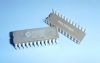
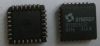
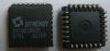
- Part Number:
- SY10E337
- Supply Ability:
- 5000
Price Break
- Qty
- 1~5000
- Unit Price
- Negotiable
- Processing time
- 15 Days
SeekIC Buyer Protection PLUS - newly updated for 2013!
- Escrow Protection.
- Guaranteed refunds.
- Secure payments.
- Learn more >>
Month Sales
268 Transactions
Payment Methods
All payment methods are secure and covered by SeekIC Buyer Protection PLUS.
Notice: When you place an order, your payment is made to SeekIC and not to your seller. SeekIC only pays the seller after confirming you have received your order. We will also never share your payment details with your seller.