DescriptionThe SY10/100E445 are integrated 4-bit serial-to-parallel data converters. The devices are designed to operate for NRZ data rates of up to 2.5Gb/s. The chip generates a divide-by-4 and a divide-by-8 clock for both 4-bit conversion and a two-chip 8-bit conversion function. The conversion ...
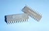
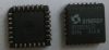
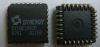
SY10/100E445: DescriptionThe SY10/100E445 are integrated 4-bit serial-to-parallel data converters. The devices are designed to operate for NRZ data rates of up to 2.5Gb/s. The chip generates a divide-by-4 and a d...
SeekIC Buyer Protection PLUS - newly updated for 2013!
268 Transactions
All payment methods are secure and covered by SeekIC Buyer Protection PLUS.
DescriptionThe SY10/100E111 are low skew 1-to-9 differential drivers designed for clock distributi...
The SY10/100E445 are integrated 4-bit serial-to-parallel data converters. The devices are designed to operate for NRZ data rates of up to 2.5Gb/s. The chip generates a divide-by-4 and a divide-by-8 clock for both 4-bit conversion and a two-chip 8-bit conversion function. The conversion sequence was chosen to convert the first serial bit to Q0, the second to Q1, etc.
Two selectable serial inputs provide a loopback capability for testing purposes when the SY10/100E445 is used in conjunction with the E446 parallel-to-serial converter.
The MODE input of SY10/100E445 is used to select the conversion mode of the device. With the MODE input LOW (or open) the device will function as a 4-bit converter. When the mode input is driven HIGH, the data on the output will change on every eighth clock cycle, thus allowing for an 8-bit conversion scheme using two E445s. When cascaded in an 8-bit conversion scheme, the devices will not operate at the 2.5Gb/s data rate of a single device. Refer to the applications section of this data sheet for more information on cascading the E445.
For lower data rate applications, SY10/100E445 is supplied for single-ended inputs. When operating at clock rates above 500MHz, differential input signals are recommended. For single-ended inputs, the VBB pin is tied to the inverting differential input and bypassed via a 0.01mF capacitor. The VBB provides the switching reference for the input differential amplifier. The VBB can also be used to AC couple an input signal.