SY89825U

Features: LVPECL or LVDS input to 22 LVPECL outputs 100K ECL compatible outputs LVDS input includes 100 termination Guaranteed AC parameters over voltage:> 2GHz fMAX (toggle)< 35ps max. ch-ch skew Low voltage operation: 2.5V, 3.3V Temperature range: 40°C to +85°C Output enable pin Available ...

product image

SY89825U Picture
SeekIC No. : 004510367 Detail

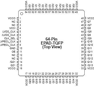
SY89825U: Features: LVPECL or LVDS input to 22 LVPECL outputs 100K ECL compatible outputs LVDS input includes 100 termination Guaranteed AC parameters over voltage:> 2GHz fMAX (toggle)< 35ps max. ch-ch ...

floor Price/Ceiling Price

Part Number:
SY89825U
Supply Ability:
5000

Price Break

  • Qty
  • 1~5000
  • Unit Price
  • Negotiable
  • Processing time
  • 15 Days
Total Cost: $ 0.00

SeekIC Buyer Protection PLUS - newly updated for 2013!

  • Escrow Protection.
  • Guaranteed refunds.
  • Secure payments.
  • Learn more >>

Month Sales

268 Transactions

Rating

evaluate  (4.8 stars)

Upload time: 2025/12/23

Payment Methods

All payment methods are secure and covered by SeekIC Buyer Protection PLUS.

Notice: When you place an order, your payment is made to SeekIC and not to your seller. SeekIC only pays the seller after confirming you have received your order. We will also never share your payment details with your seller.
Product Details

Description


Features:

LVPECL or LVDS input to 22 LVPECL outputs
100K ECL compatible outputs
LVDS input includes 100 termination
Guaranteed AC parameters over voltage:
> 2GHz fMAX (toggle)
< 35ps max. ch-ch skew
Low voltage operation: 2.5V, 3.3V
Temperature range: 40°C to +85°C
Output enable pin
Available in a 64-Pin EPAD-TQFP


Application

High-performance PCs
Workstations
Parallel processor-based systems
Other high-performance computing
Communications


Pinout

  Connection Diagram


Specifications

Symbol Rating Value Unit
VCCI/ VCCO VCC Pin Potential to Ground Pin 0.5 to +4.0 V
VIN Input Voltage 0.5 to VCCI V
IOUT DC Output Current -50
mA
TSTORE Storage Temperature Range -65 to +150 °C
JA Package Thermal Resistance (Junction-to-Ambient)
With exposed pad soldered to GND Still-Air (multi-layer PCB)
200lfpm (multi-layer PCB)
500lfpm (multi-layer PCB)
23
18
25
°C/W
°C/W
°C/W
Exposed pad not soldered to GND Still-Air (multi-layer PCB)
200lfpm (multi-layer PCB)
500lfpm (multi-layer PCB)
44
36
30
°C/W
°C/W
°C/W
JC Package Thermal Resistance
(Junction-to-Case)
4.3 °C/W


Description

The SY89825U is a High Performance Bus Clock Driver with 22 differential LVPECL output pairs. This part is designed for use in low voltage (2.5V, 3.3V) applications which require a large number of outputs to drive precisely aligned, ultra low skew signals to their destination. The input is multiplexed from either LVDS or LVPECL by the CLK_SEL pin. The LVDS input includes a 100 internal termination, thus eliminating the need for external termination. The Output Enable (OE) is synchronous so that the outputs will only be enabled/disabled when they are already in the LOW state. This eliminates any chance of generating a runt clock pulse when the device is enabled/ disabled as can happen with an asynchronous control.

The SY89825U features low pin-to-pin skew (35ps max.) -performance previously unachievable in a standard product having such a high number of outputs. The SY89825U is available in a single space saving package which provides a lower overall cost solution. In addition, a single chip solution improves timing budgets by eliminating the multiple device solution with their corresponding large part-to-part skew.


Customers Who Bought This Item Also Bought

Margin,quality,low-cost products with low minimum orders. Secure your online payments with SeekIC Buyer Protection.
Prototyping Products
DE1
LED Products
Boxes, Enclosures, Racks
Resistors
Power Supplies - Board Mount
Static Control, ESD, Clean Room Products
View more