Si6924EDQ

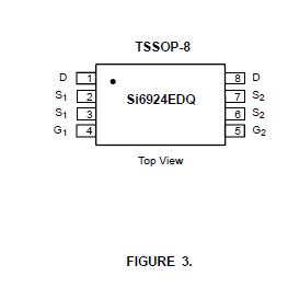
Features: · Low rDS(on)· VGS Max Rating: 14 V· Exceeds 2-kV ESD Protection· Low Profile TSSOP-8 Package· rDS(on) Rating at 2.5-V VGS· 28-V VDS Rated· Symetrical Voltage Blocking (Off Voltage)PinoutSpecifications Parameter Symbol N-Channel Unit Drain-Source Voltage VDS - to + V Gat...

product image

Si6924EDQ Picture
SeekIC No. : 004490590 Detail

Si6924EDQ: Features: · Low rDS(on)· VGS Max Rating: 14 V· Exceeds 2-kV ESD Protection· Low Profile TSSOP-8 Package· rDS(on) Rating at 2.5-V VGS· 28-V VDS Rated· Symetrical Voltage Blocking (Off Voltage)PinoutS...

floor Price/Ceiling Price

Part Number:
Si6924EDQ
Supply Ability:
5000

Price Break

  • Qty
  • 1~5000
  • Unit Price
  • Negotiable
  • Processing time
  • 15 Days
Total Cost: $ 0.00

SeekIC Buyer Protection PLUS - newly updated for 2013!

  • Escrow Protection.
  • Guaranteed refunds.
  • Secure payments.
  • Learn more >>

Month Sales

268 Transactions

Rating

evaluate  (4.8 stars)

Upload time: 2025/12/25

Payment Methods

All payment methods are secure and covered by SeekIC Buyer Protection PLUS.

Notice: When you place an order, your payment is made to SeekIC and not to your seller. SeekIC only pays the seller after confirming you have received your order. We will also never share your payment details with your seller.
Product Details

Description


Features:

· Low rDS(on)
· VGS Max Rating: 14 V
· Exceeds 2-kV ESD Protection
· Low Profile TSSOP-8 Package
· rDS(on) Rating at 2.5-V VGS
· 28-V VDS Rated
· Symetrical Voltage Blocking (Off Voltage)


Pinout

  Connection Diagram


Specifications

Parameter Symbol N-Channel Unit
Drain-Source Voltage VDS - to + V
Gate-Source Voltage VGS ±14
Continuous Drain Current (TJ = 150)a, b TA = 25 ID ±4.6 A
TA = 70 ±3.7
Pulsed Drain Current IDM ±20
Continuous Source Current (Diode Conduction)a, b IS 1.25
Maximum Power Dissipationa, b TA = 25 PD 1.1 W
TA = 70 0.72
Operating Junction and Storage Temperature Range TJ, Tstg -55 to 150 /W


Description

The Si6924EDQ is a dual n-channel MOSFET with ESD protection and gate over-voltage protection circuitry incorporated into the MOSFET. The device is designed for use in Lithium Ion battery pack circuits. The common-drain contsruction takes advantage of the typical battery pack topology, allowing a further reduction of the device's on-resistance. The 2-stage input protection circuit is a unique design, consisting of two stages of back-to-back zener diodes separated by a resistor. The first stage diode is designed to absorb most of the ESD energy. The second stage diode is designed to protect the gate from any remaining ESD energy and over-voltages above the gates inherent safe operating range. The series resistor used to limit the current through the second stage diode during over voltage conditions has a maximum value which limits the input current to 10 mA @ 14 V and the maximum toff to 12 s. The Si6924EDQ has been optimized as a battery or load switch in Lithium Ion applications with the advantage of both a 2.5-V rDS(on) rating and a safe 14-V gate-to-source maximum rating.


Customers Who Bought This Item Also Bought

Margin,quality,low-cost products with low minimum orders. Secure your online payments with SeekIC Buyer Protection.
Line Protection, Backups
LED Products
Crystals and Oscillators
Undefined Category
Connectors, Interconnects
Test Equipment
View more