DescriptionN-Channel 1.2-V (G-S) MOSFET The Si8424DB is designed as one kind of N-channel 1.2V (G-S) MOSFETs with typical applications for low threshold load switch for portable devices with low power consumption and increased battery life and ultra low voltage load switch.Si8424DB has three feat...
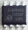
Si8424DB: DescriptionN-Channel 1.2-V (G-S) MOSFET The Si8424DB is designed as one kind of N-channel 1.2V (G-S) MOSFETs with typical applications for low threshold load switch for portable devices with low po...
SeekIC Buyer Protection PLUS - newly updated for 2013!
268 Transactions
All payment methods are secure and covered by SeekIC Buyer Protection PLUS.
US $1.55 - 1.55 / Piece
Isolator Interface IC 1.0 kV Bidirectional I2C Isolator 1.7MHz
The Si8424DB is designed as one kind of N-channel 1.2V (G-S) MOSFETs with typical applications for low threshold load switch for portable devices with low power consumption and increased battery life and ultra low voltage load switch.
Si8424DB has three features. (1)TrenchFET power MOSFET. (2)Industry first 1.2V rated MOSFET. (3)Ultra small MICRO FOOT chipscale packaging reduces footprint area, profile (0.62mm) and on-resistance per footprint area. Those are all the main features.
Some absolute maximum ratings of Si8424DB have been concluded into several points as follow. (1)Its drain-source voltage would be 8V. (2)Its gate to source voltage would be +/-5V. (3)Its continuous drain current would be 12.2A at Tc=25°C and would be 9.8A at Tc=70°C. (4)Its pulse drain current would be 20A. (5)Its continuous source-drain diode current would be 5.2A at Tc=25°C. (6)Its maximum power dissipation would be 6.25W at Tc=25°C and would be 4W at Tc=70°C. (7)Its operating junction temperature range would be from -55°C to 150°C. (8)Its storage temperature range would be from -55°C to 150°C. (9)Its package reflow conditions would be 260°C. It should be noted that stresses above those listed in absolute maximum ratings may cause permanent damage to device.
Also some electrical characteristics of Si8424DB are concluded as follow. (1)Its drain-source breakdown voltage would be min 8V. (2)Its Vds temperature coefficient would be typ 8.9mV/°C. (3)Its Vgs(th) temperature coefficient would be typ -2.5mV/°C. (4)Its gate to source threshold voltage would be min 0.35V and max 1.0V. (5)Its gate to source leakage would be max 100nA. (6)Its zero gate voltage drain current would be max 1uA and would be max 10uA at Tj=70°C. (7)Its on-state drain current would be min 20A. (8)Its drain to source on-state resistance would be typ 0.025ohms and max 0.031ohms at Vgs=4.5V and Id=1A and would be typ 0.027ohms and max 0.033ohms at Vgs=2.5V and Id=1A. And so on. At present we have not got so much information about this IC and we would try hard to get more information about it. If you have any question or suggestion or want to know more information please contact us for details. Thank you!