T0370

Features: • High power added efficiency• Excellent ACP and ALT• Three quiescent current states• CMOS compatible state logic inputs• Internally matched input and output• Low leakage current• Single +3.0 V operationApplicationThe application circuit for the ...

product image

T0370 Picture
SeekIC No. : 004510753 Detail

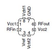
T0370: Features: • High power added efficiency• Excellent ACP and ALT• Three quiescent current states• CMOS compatible state logic inputs• Internally matched input and output&...

floor Price/Ceiling Price

Part Number:
T0370
Supply Ability:
5000

Price Break

  • Qty
  • 1~5000
  • Unit Price
  • Negotiable
  • Processing time
  • 15 Days
Total Cost: $ 0.00

SeekIC Buyer Protection PLUS - newly updated for 2013!

  • Escrow Protection.
  • Guaranteed refunds.
  • Secure payments.
  • Learn more >>

Month Sales

268 Transactions

Rating

evaluate  (4.8 stars)

Upload time: 2024/4/26

Payment Methods

All payment methods are secure and covered by SeekIC Buyer Protection PLUS.

Notice: When you place an order, your payment is made to SeekIC and not to your seller. SeekIC only pays the seller after confirming you have received your order. We will also never share your payment details with your seller.
Product Details

Description


Features:

• High power added efficiency
• Excellent ACP and ALT
• Three quiescent current states
• CMOS compatible state logic inputs
• Internally matched input and output
• Low leakage current
• Single +3.0 V operation


Application

The application circuit for the T0370 is very simple since most of the critical components are included inside the module. There are several important considerations when using the module in a phone design.

First of all, it is important that the source impedance of the VCC power supply is very low.This is because the high current demand during the modulation peaks of the CDMA waveform can introduce voltage ripple at the symbol rate that will introduce additional intermodulation distortion or adjacent channel power distortion at the output of the power amplifier. If the power amplifier has a quiescent current of 100 mA and a peak current demand in excess of 1 A, it is possible to see 900 mA change in the current required from VCC as the modulated signal moves from one extreme to the other. If the power supply source impedance is 1 , the resulting voltage ripple would be 0.9 V which would cause the amplifier to fail in ACP requirements. Generally, the power supply source impedance should be kept as low as possible, preferably below 0.1 ohms total. Most battery technologies used in cellular telephones will support a low source impedance, but it may be necessary to supplement this in some designs with an low ESR capacitor. Ceramic or tantalum capacitors of approximately 10 micro-farads work well for this requirement.

The application circuit includes 100 nF capacitors at each of the PA control lines and VCC lines to ensure proper RF bypassing. Depending on the phone board layout and circuit bypassing in other areas of the phone, some of these components may not be necessary. There are a number of VCO signals and IF signals used in a given phone design, so it is important to protect the PA module from interfering signals and to limit any interference coming from the PA itself. Care should be taken when removing any of the RF bypassing components.

One final area of concern is with excessive bypassing. If too large a value of bypassing capacitor is used on any of the control lines, it could reduce the frequency response of that control line to the point where a specification failure could occur. Please be sure that the logic lines and regulated supply lines driving the power amplifier control lines are adequate to supply peak current requirements of the bypassing capacitors chosen on the control lines.


Pinout

  Connection Diagram


Specifications

Parameter
Symbol
Value
Unit
Power supply voltage, no RF applied
VCC1, VCC2
- 0.5 to + 6.0
VDC
Power supply voltage, RF applied
VCC1, VCC2
- 0.5 to + 5.0
VDC
Bias reference voltages and bias control
voltages (Pins 3, 4, and 8 respectively)
VREF, VCtrl1, VCtrl2
- 0.5 to + 5.0
VDC
Power dissipation
PDISS
2.5
W
Case temperature, survival
TC
-40 to +100
°C
Storage temperature
Tstg
-40 to +150
°C
DC blocked RF output
RFOUT
-20 to +20
VDC
DC grounded RF input ( no DC voltages)
RFIN
0 to 0
VDC
Note: The part may not survive all maximums applied simultaneously.


Description

The T0370 is a 6 mm × 6 mm 3-V CDMA/AMPS cell-band power-amplifier module designed for use in mobile phones. The module incorporates a SiGe HBT two-stage CDMA / AMPS power-amplifier die. The T0370 is 50-Ohm matched on the input and output allowing the device to be used with minimal external circuitry. Its RF performance meets the requirements for products designed to the IS-95A and B and IS-98 standards.

The T0370 gives excellent RF performance with low current consumption resulting in longer talk times in portable applications. The module features three quiescent current states to minimize current consumption for each output power level. The module has a small 6 mm × 6 mm footprint to allow use in compact phone design.


Customers Who Bought This Item Also Bought

Margin,quality,low-cost products with low minimum orders. Secure your online payments with SeekIC Buyer Protection.
LED Products
Cable Assemblies
Audio Products
Crystals and Oscillators
Soldering, Desoldering, Rework Products
View more