T7689

Features: ` Four fully integrated T1 line interfaces` Includes all driver, receiver, equalization, clockrecovery, and jitter attenuation functions` Ultralow power consumption` Robust operation for increased system margin` High interference immunity` On-chip transmit equalization for improved sensi...

product image

T7689 Picture
SeekIC No. : 004511486 Detail

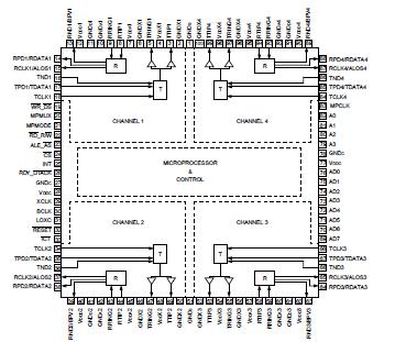
T7689: Features: ` Four fully integrated T1 line interfaces` Includes all driver, receiver, equalization, clockrecovery, and jitter attenuation functions` Ultralow power consumption` Robust operation for i...

floor Price/Ceiling Price

Part Number:
T7689
Supply Ability:
5000

Price Break

  • Qty
  • 1~5000
  • Unit Price
  • Negotiable
  • Processing time
  • 15 Days
Total Cost: $ 0.00

SeekIC Buyer Protection PLUS - newly updated for 2013!

  • Escrow Protection.
  • Guaranteed refunds.
  • Secure payments.
  • Learn more >>

Month Sales

268 Transactions

Rating

evaluate  (4.8 stars)

Upload time: 2024/4/28

Payment Methods

All payment methods are secure and covered by SeekIC Buyer Protection PLUS.

Notice: When you place an order, your payment is made to SeekIC and not to your seller. SeekIC only pays the seller after confirming you have received your order. We will also never share your payment details with your seller.
Product Details

Description


Features:

Four fully integrated T1 line interfaces
Includes all driver, receiver, equalization, clock recovery, and jitter attenuation functions
Ultralow power consumption
Robust operation for increased system margin
High interference immunity
On-chip transmit equalization for improved sensitivity
Low-impedance drivers for reduced power consumption
Selectable transmit or receive, jitter attenuation/clock smoothing
3-state transmit drivers
High-speed, microprocessor interface
Automatic transmit monitor function
Per-channel powerdown
For use in systems that are compliant with AT&T CB119; TR-TSY-000170, TR-TSY-000009, TRTSY-000499, TR-TSY-000253; ANSI T1.102 and T1.403
Common transformer for transmit/receive
Fine-pitch (25 mil spacing) surface-mount package, 100-pin bumpered quad flat pack
40°C to +85°C operating temperature range


Application

·  SONET/SDH multiplexers
·  Asynchronous multiplexers (M13)
·  Digital access cross connects (DACs)
·  Channel banks
·  Digital radio base stations, remote wireless modules
·  PBX interfaces


Pinout

  Connection Diagram


Specifications

Parameter
Min
Max
Unit
dc Supply Voltage
-0.5
6.5
V
Storage Temperature
-65
125
Maximum Voltage (digital pins) with Respect to VDDD
-
0.5
V
Minimum Voltage (digital pins) with Respect to GNDD
-0.5
-
V
Maximum Allowable Voltages (RTIP[1-4], RRING[1-4])
with Respect to VDD
-
0.5
V
Minimum Allowable Voltages (RTIP[1-4], RRING[1-4])
with Respect to GND
-0.5
-
V
 
Stresses in excess of the absolute maximum ratings can cause permanent or latent damage to the device. These are absolute stress ratings only. Functional operation of the device is not implied at these or any other conditions in excess of those given in the operational sections of this device specification. Exposure to absolute maximum ratings for extended periods can adversely affect device reliability.


Description

The T7689 is a fully integrated quad line interface containing four transmit and receive channels for use in North American (T1/DS1) applications. The device has many of the same functions as the Lucent Technologies Microelectronics Group T7290A and provides additional flexibility for the system designer.

Included is a parallel microprocessor interface that allows the user to define the architecture, initiate loopbacks, and monitor alarms. The T7689 interface is compatible with many commercially available microprocessors.

The receiver performs clock and data recovery using a fully integrated digital phase-locked loop. This T7689 conditions that are common when recovering sparse data patterns with analog phase-locked loops. Equalization circuitry in the receiver guarantees a high level of interference immunity. As an option, the raw sliced data (no retiming) can be output on the receive data pins.

Transmit equalization is implemented with lowimpedance output drivers that provide shaped waveforms to the transformer, guaranteeing template conformance. The quad T7689 device will interface to the digital cross connect (DSX) at lengths of up to 655 ft. for DS1 operation.

A selectable jitter attenuator may be placed in the receive signal path for low-andwidth linesynchronous applications, or it may be placed in the transmit path for multiplexer applications where DS1 signals are demultiplexed from higher rate signals. The jitter attenuator will perform the clock smoothing required on the resulting demultiplexed gapped clock.


Customers Who Bought This Item Also Bought

Margin,quality,low-cost products with low minimum orders. Secure your online payments with SeekIC Buyer Protection.
Industrial Controls, Meters
Sensors, Transducers
Test Equipment
Optical Inspection Equipment
Connectors, Interconnects
Discrete Semiconductor Products
View more