Available Set Gain
:
Common Mode Rejection Ratio (Min)
:
Operating Supply Voltage
:
Maximum Power Dissipation
:
Mounting Style
: SMD/SMT
THD plus Noise
: 0.025 %
Packaging
: Tube
Maximum Operating Temperature
: + 70 C
Output Type
: 2-Channel Stereo
Product
: Class-AB
Output Power
: 50 W
Supply Current
: 1 mA
Package / Case
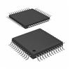
: HTSSOP-56
DescriptionThe TAS5112ADFD belongs to TAS5112A. The TAS5112A is a high-performance, integrated stereo digital amplifier power stage designed to drive 6-Ω speakers at up to 50 W per channel. The device incorporates TI's PurePath DigitalTM technology and is used with a digital audio PWM processor (TAS50XX) and a simple passive demodulation filter to deliver high-quality, high-efficiency, true-digital audio amplification. The efficiency of this digital amplifier is typically 90%, reducing the size of both the power supplies and heatsinks needed. Overcurrent protection of the TAS5112ADFD, overtemperature protection, and undervoltage protection are built into the TAS5112A, safeguarding the device and speakers against fault conditions that could damage the system.
The features of TAS5112ADFD are (1)50 W per channel (BTL) into 6 Ω (Stereo); (2)95-dB dynamic range with TAS5026; (3) less than 0.2% THD+N (50 W RMS into 6 Ω); (4)self-protecting design (undervoltage, overtemperature and short conditions) with error reporting; (5)less than 0.1% THD+N (1 W RMS Into 6 Ω); (6)EMI compliant when used with recommended system design; (7)power efficiency typically 90% into 6-Ω load; (8)internal gate drive supply voltage regulator. The TAS5112A can be used in DVD receiver; home theatre; Mini/Micro component systems; internet music appliance.
The absolute maximum ratings of TAS5112ADFD (over operating free-air temperature range unless otherwise noted(1: Stresses beyond those listed under "absolute maximum ratingsmay cause permanent damage to the device. These are stress ratings only, and functional operation of the device at these or any other conditions beyond those indicated under "recommended operating conditions" is not implied. Exposure to absolute-maximum-rated conditions for extended periods may affect device reliability.))are (1)DVDD TO DGND: -0.3 V to 4.2 V; (2)GVDD TO GND: 33.5 V; (3)PVDD_X TO GND (dc voltage): 33.5 V; PVDD_X TO GND (spike voltage(2: The duration of voltage spike should be less than 100 ns; see application note SLEA025.)): 48 V; (4)OUT_X TO GND (dc voltage): 33.5 V; (5)OUT_X TO GND (spike voltage(2)): 48 V; (6)BST_X TO GND (dc voltage): 48 V; (7)BST_X TO GND (spike voltage(2)): 53 V; (8)GREG TO GND (3: GREG is treated as an input when the GREG pin is overdriven by GVDD of 12 V.): 14.2 V; (9)PWM_XP, RESET, M1, M2, M3, SD,OTW of the TAS5112ADFD: -0.3 V to DVDD + 0.3 V; (10)maximum operating junction temperature, TJ: -40°C to 150°C; (11)storage temperature: -40°C to 125°C.

 TAS5112ADFD Data Sheet