TC5020BP

Features: SpecificationsDescriptionThe TC5020BP is designed as C2MOS digital integrated circuit silicon monolithic. It contains six circuits of level converters which convert the signals from low power supply voltage logical systems to the logical signals for high power supply voltage C2MOS system...

product image

TC5020BP Picture
SeekIC No. : 004513818 Detail

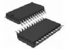
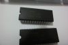
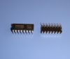
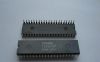
TC5020BP: Features: SpecificationsDescriptionThe TC5020BP is designed as C2MOS digital integrated circuit silicon monolithic. It contains six circuits of level converters which convert the signals from low po...

floor Price/Ceiling Price

Part Number:
TC5020BP
Supply Ability:
5000

Price Break

  • Qty
  • 1~5000
  • Unit Price
  • Negotiable
  • Processing time
  • 15 Days
Total Cost: $ 0.00

SeekIC Buyer Protection PLUS - newly updated for 2013!

  • Escrow Protection.
  • Guaranteed refunds.
  • Secure payments.
  • Learn more >>

Month Sales

268 Transactions

Rating

evaluate  (4.8 stars)

Upload time: 2024/4/27

Payment Methods

All payment methods are secure and covered by SeekIC Buyer Protection PLUS.

Notice: When you place an order, your payment is made to SeekIC and not to your seller. SeekIC only pays the seller after confirming you have received your order. We will also never share your payment details with your seller.
Product Details

Description


Features:


Specifications


Description

The TC5020BP is designed as C2MOS digital integrated circuit silicon monolithic. It contains six circuits of level converters which convert the signals from low power supply voltage logical systems to the logical signals for high power supply voltage C2MOS systems.

Some absolute maximum ratings of TC5020BP have been concluded into several points as follow. The first one is about its DC supply voltage which would be from Vss-0.5V to Vss+20V for Vdd and would be from Vss-0.5V to Vdd+0.5V for Vcc. The second one is about its input voltage which would be from Vss-0.5V to Vcc+0.5V. The third one is about its output voltage which would be from Vss-0.5V to Vdd+0.5V. The fourth one is about its DC input current which would be +/-10mA. The fifth one is about its power dissipation which would be 300mW. The sixth one is about its storage temperature range which would be from -65°C to 150°C. The seventh one is about its lead temperature / time which would be 260°C / 10sec.

And some electrical characteristics about TC5020BP. For Vdd=5V the second one is about its high level output voltage which would be min 4.95V and typ 5.00V. The second one is about its low level output voltage which would be typ 0.00V and max 0.05V. The third one is about its high level output current which would be min -0.16mA. The fourth one is about its low level output current which would be min 0.44mA. The fifth one is about its high level input voltage which would be min 4.0V. The sixth one is about its low level input voltage which would be max 1.0V. The seventh one is about its high level input current which would be max 0.3uA. The eighth one is about its low level input current which would be max -0.3uA. The ninth one is about its quiescent current consumption which would be typ 0.2mA and max 0.48mA with conditio of Vin=Vdd and it would be typ 0.001ua and max 1.0uA with condition of Vin=Vss. And so on. For more information please contact us.


Customers Who Bought This Item Also Bought

Margin,quality,low-cost products with low minimum orders. Secure your online payments with SeekIC Buyer Protection.
Resistors
Circuit Protection
Crystals and Oscillators
Programmers, Development Systems
Inductors, Coils, Chokes
View more